Introduction
Introducing the Mimas AU-Plus Development Module – Your Gateway to FPGA Innovation!
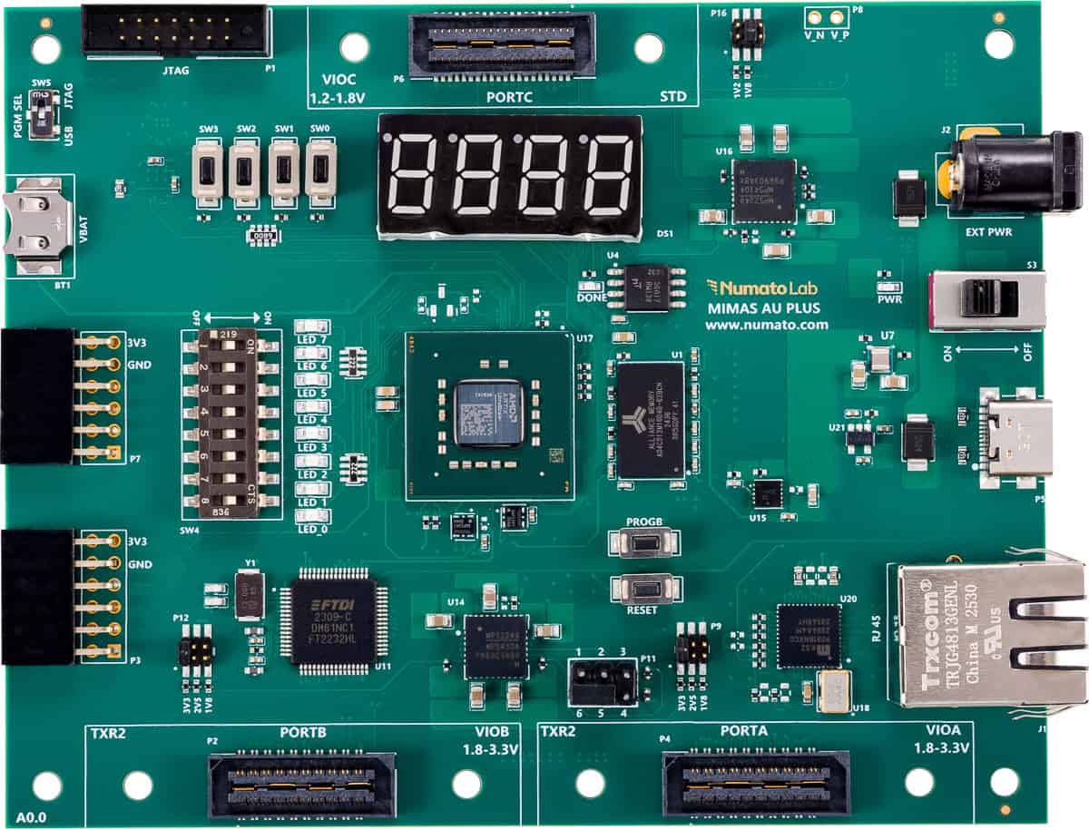
Mimas AU-Plus Development Module is an easy-to-use FPGA Development Module featuring Artix Ultrascale+ FPGA (XCAU7P-1SBVC484 package). The FT2232H brings versatile USB-to-serial connectivity, while DDR4 support enhances data processing efficiency. The inclusion of Gigabit Ethernet facilitates seamless networking, opening doors to IoT and cloud computing applications. Storage is swift and reliable with QSPI flash. The addition of SYZYGY and PMOD connectors enhances flexibility, allowing easy interfacing with sensors and peripherals for customized projects.
In essence, the AU-Plus Development Module is a compact, feature-rich solution for FPGA development, empowering both seasoned developers and enthusiasts to explore limitless possibilities in embedded systems and digital design.
Board Features
- Device: AMD Artix Ultrascale+ FPGA (XCAU7P-1SBVC484).
- SDRAM – DDR4.
- Flash Memory: 128 Mb SPI flash memory.
- 1 x Gigabit Ethernet PHY.
- FTDI FT2232H based host interface.
- 100MHz CMOS oscillator (Fabric clock).
- 100MHz DDR4 Reference Clock.
- FPGA configuration via JTAG and USB.
- 2x TXR-2 and 1x standard SYZYGY connector.
- 2x PMOD.
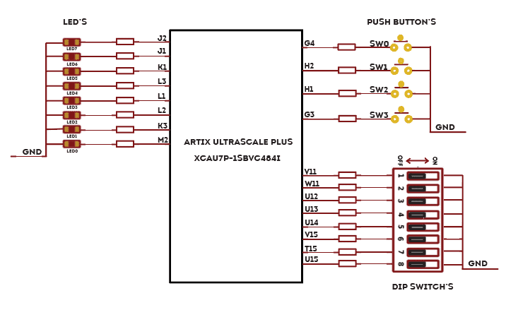
- 8 LEDs, 4 Push Buttons, 8 DIP switches and 7 Segment display for user-defined purposes.
Application
- Digital Signal Processing (DSP) Applications
- Networked Systems and IoT Solutions
- Data Storage and Retrieval
- High-Speed Storage Solutions
- Embedded Systems Development
- Prototyping and Rapid Development
- Educational and Research Initiatives
- Robotics and Automation
How to use Mimas AU-Plus Development Module
The following sections describe in detail how to use this module.
Hardware Accessories Required
- 5V DC Power Supply.
- Xilinx Platform Cable USB II JTAG debugger.
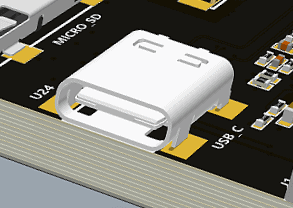
- USB Type C cable.
Connection Diagram
USB Interface
DC Power Supply
The board is configured to use power from DC power supply by connecting it to the External DC Jack. Please refer to the marking on the board for more details. The external power supply should be 5V, with sufficient current rating.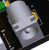
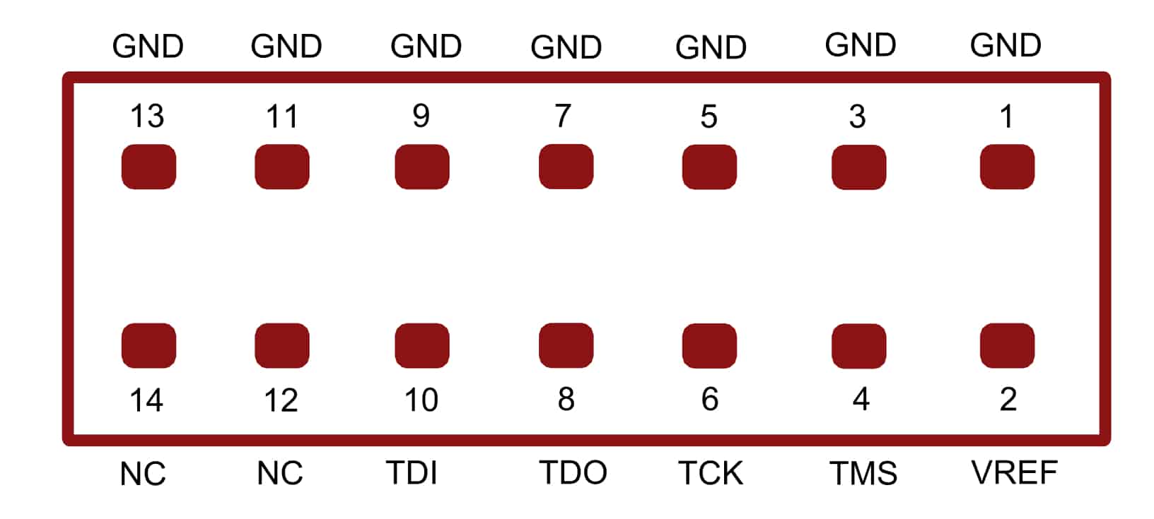
JTAG Connector
PROG_B and Reset Buttons
PROG_B Button
Mimas AU-Plus features a Push-button S1 normally meant to be used as a “PROG_B” signal for configuration reset. Push-button S1 is connected to FPGA pin C7. For enabling manual configuration reset, push-button S1 is connected to GND. The user can reconfigure the FPGA manually, by pressing this push-button S1.
“PROG_B” is an active-low input pin (pulled up with 4.7K external resistor) to the FPGA and it controls the configuration logic. When the PROG_B pin is de-asserted, resets the FPGA and initializes the new configuration.
Reset Button
Mimas AU-Plus features a Push-button S2 normally meant to be used as a “Reset” signal for designs running on FPGA. Push-button S2 is connected to FPGA pin U14. Push-button S2 is active-high. This pushbutton can also be used for any other input and is not just limited to be used as a Reset signal.
LED, Push Button and Dip Switch
7-Segment LED Display
The board features four 7-segment LED displays. Each module can be separately turned on and off with the four switching transistors.
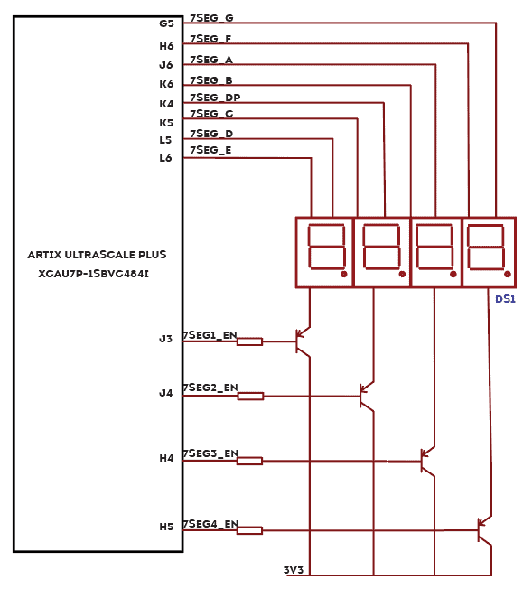
Note: All signals (a, b, c, d, e, f, g, dot, enable 1, enable 2, enable 3, enable 4) used for controlling 7-Segment display are active-low signals.
For example, to display “8” on display-2, users should set Enable 2 to 0 and drive signals a, b, c, d, e, and f to 0, while setting all other signals to 1.
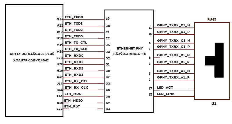
Gigabit Ethernet
The KSZ9031RNX is a completely integrated triple-speed (10BASE-T/100BASE-TX/1000BASE-T) Ethernet physical layer transceiver for transmission and reception of data. It provides the Reduced Gigabit Media Independent Interface (RGMII) for direct connection to RGMII MACs in Gigabit Ethernet processors and switches for data transfer at 10/100/1000 Mbps.
SPI FLASH
The Mimas AU-Plus Development Module has 128 Mbit of Quad SPI flash memory. It is a serial NOR flash which operates at the voltage of 1.8 V. It serves as the default primary boot device.
DDR4
Mimas AU-Plus Development Module uses DDR4(AS4C512M16D4B-62BCN) which is a high-speed dynamic random-access memory internally configured as an eight-bank DRAM. The DDR4 SDRAM uses an 8n-prefetch architecture to achieve high-speed operation. The 8n-prefetch architecture is combined with an interface designed to transfer two data words per clock cycle at the I/O pins. DDR4 is connected to the bank 66 of Artix Ultrascale Plus FPGA.
Reference clock
Fabric clock
| Clock pins | FPGA pins |
|---|---|
| REF_CLK_P | K18 |
| REF_CLK_N | J18 |
DDR4 Reference Clock
| Clock pins | FPGA pins |
|---|---|
| DDR4_REFCLK_P | B14 |
| DDR4_REFCLK_N | B15 |
FT2232H - Artix Ultrascale Plus (1SBVC484) FPGA Connection Details
| FTDI Pin No. | Pin Function | Signal name | FPGA pins |
|---|---|---|---|
| 38 | FTDI-D0 | IO_L6P_HDGC_84 | Y6 |
| 39 | FTDI-D1 | IO_L5N_HDGC_84 | AB7 |
| 40 | FTDI-D2 | IO_L5P_HDGC_84 | AA7 |
| 41 | FTDI-D3 | IO_L4N_AD12N_84 | AB8 |
| 43 | FTDI-D4 | IO_L4P_AD12N_84 | AA8 |
| 44 | FTDI-D5 | IO_L2N_AD14N_84 | AB9 |
| 45 | FTDI-D6 | IO_L3P_AD13P_84 | Y10 |
| 46 | FTDI-D7 | IO_L1N_AD15N_84 | AB10 |
| 48 | FTDI-RXF# | IO_L8P_HDGC_84 | V9 |
| 52 | FTDI-TXE# | IO_L7N_HDGC_84 | Y8 |
| 53 | FTDI-RD# | IO_L3N_AD13N_84 | Y9 |
| 54 | FTDI-WR# | IO_L1P_AD15P_84 | AA11 |
| 55 | FTDI-SIWUA | IO_L2P_AD14P_84 | AA10 |
SYZYGY Connectors
SYZYGY PORT A
| Pin No. On The Header | Pin Name | Signal name | FPGA Pin | Pin No. On The Header | Pin Name | Signal name | FPGA Pin |
|---|---|---|---|---|---|---|---|
| 1 | SYZYGY_PORT_SCL | IO_L9P_AD11P_84 | U10 | 2 | VIN | ||
| 3 | SYZYGY_PORT_SDA | IO_L9N_AD11N_84 | V10 | 4 | GND | ||
| 5 | SZG_PORTA_RX0_P | MGTHRXP0_124 | AA21 | 6 | SZG_PORTA_TX0_P | MGTHTXP0_124 | AB19 |
| 7 | SZG_PORTA_RX0_N | MGTHRXN0_124 | AA22 | 8 | SZG_PORTA_TX0_N | MGTHTXN0_124 | AB20 |
| 9 | SZG_PORTA_RX1_P | MGTHRXP1_124 | W21 | 10 | SZG_PORTA_TX1_P | MGTHTXP1_124 | Y19 |
| 11 | SZG_PORTA_RX1_N | MGTHRXN1_124 | W22 | 12 | SZG_PORTA_TX1_N | MGTHTXN1_124 | Y20 |
| 13 | SZG_PORTA_REFCLK_P | MGTREFCLK0P_124 | AA17 | 14 | SZG_PORTA_S0 | IO_L10P_AD2P_86 | B5 |
| 15 | SZG_PORTA_REFCLK_N | MGTREFCLK0N_124 | AA18 | 16 | SZG_PORTA_S1 | IO_L10N_AD2N_86 | A5 |
| 17 | SZG_PORTA_S2 | IO_L2P_AD10P_86 | F3 | 18 | SZG_PORTA_S3 | IO_L9P_AD3P_86 | C5 |
| 19 | SZG_PORTA_S4 | IO_L2N_AD10N_86 | E3 | 20 | SZG_PORTA_S5 | IO_L9N_AD3N_86 | B4 |
| 21 | SZG_PORTA_S6 | IO_L4P_AD8P_86 | G2 | 22 | SZG_PORTA_S7 | IO_L11P_AD1P_86 | B3 |
| 23 | SZG_PORTA_S8 | IO_L4N_AD8N_86 | F2 | 24 | SZG_PORTA_S9 | IO_L11N_AD1N_86 | A3 |
| 25 | SZG_PORTA_S10 | IO_L3P_AD9P_86 | E4 | 26 | SZG_PORTA_S11 | IO_L12P_AD0P_86 | B2 |
| 27 | SZG_PORTA_S12 | IO_L3N_AD9N_86 | D3 | 28 | SZG_PORTA_S13 | IO_L12N_AD0N_86 | A2 |
| 29 | SZG_PORTA_S14 | IO_L5P_HDGC_D7P_86 | F1 | 30 | SZG_PORTA_S15 | IO_L8P_HDGC_AD4P_86 | D4 |
| 31 | SZG_PORTA_S16 | IO_L5N_HDGC_AD7N_86 | E1 | 32 | SZG_PORTA_S17 | IO_L8N_HDGC_AD4N_86 | C4 |
| 33 | SZG_PORTA_P2C_CLK_P | IO_L6P_HDGC_AD6P_86 | D1 | 34 | SZG_PORTA_C2P_CLK_P | IO_L7P_HDGC_AD5P_86 | D2 |
| 35 | SZG_PORTA_P2C_CLK_N | IO_L6N_HDGC_AD6N_86 | C1 | 36 | SZG_PORTA_C2P_CLK_N | IO_L7N_HDGC_AD5N_86 | C2 |
| 37 | RSVD | 38 | RSVD | E5 | |||
| 39 | VIOA | 40 | VDD3V3 |
SYZYGY PORT B
| Pin No. On The Header | Pin Name | Signal name | FPGA Pins | Pin No. On The Header | Pin Name | Signal name | FPGA Pins |
|---|---|---|---|---|---|---|---|
| 1 | SYZYGY_PORT_SCL | IO_L9P_AD11P_84 | U10 | 2 | VIN | ||
| 3 | SYZYGY_PORT_SDA | IO_L9N_AD11N_84 | V10 | 4 | GND | ||
| 5 | SZG_PORTB_RX2_P | MGTHRXP2_124 | U21 | 6 | SZG_PORTB_TX2_P | MGTHTXP2_124 | V19 |
| 7 | SZG_PORTB_RX2_N | MGTHRXN2_124 | U22 | 8 | SZG_PORTB_TX2_N | MGTHTXN2_124 | V20 |
| 9 | SZG_PORTB_RX3_P | MGTHRXP3_124 | R21 | 10 | SZG_PORTB_TX3_P | MGTHTXP3_124 | T19 |
| 11 | SZG_PORTB_RX3_N | MGTHRXN3_124 | R22 | 12 | SZG_PORTB_TX3_N | MGTHTXN3_124 | T20 |
| 13 | SZG_PORTB_REFCLK_P | MGTREFCLK1P_124 | U17 | 14 | SZG_PORTB_S0 | IO_L8P_HDGC_104 | Y5 |
| 15 | SZG_PORTB_REFCLK_N | MGTREFCLK1N_124 | U18 | 16 | SZG_PORTB_S1 | IO_L8N_HDGC_104 | AA5 |
| 17 | SZG_PORTB_S2 | IO_L2P_AD14P_104 | AB3 | 18 | SZG_PORTB_S3 | IO_L9P_AD11P_104 | U5 |
| 19 | SZG_PORTB_S4 | IO_L2N_AD14N_104 | AB2 | 20 | SZG_PORTB_S5 | IO_L9N_AD3N_86 | B4 |
| 21 | SZG_PORTB_S6 | IO_L3P_AD13P_104 | Y3 | 22 | SZG_PORTB_S7 | IO_L10P_AD10P_104 | U4 |
| 23 | SZG_PORTB_S8 | IO_L3N_AD13N_104 | AA3 | 24 | SZG_PORTB_S9 | IO_L10N_AD10N_104 | V4 |
| 25 | SZG_PORTB_S10 | IO_L4P_AD12P_104 | AA2 | 26 | SZG_PORTB_S11 | IO_L11P_AD9P_104 | U3 |
| 27 | SZG_PORTB_S12 | IO_L4N_AD12N_104 | AA1 | 28 | SZG_PORTB_S13 | IO_L11N_AD9N_104 | V2 |
| 29 | SZG_PORTB_S14 | IO_L5P_HDGC_104 | W1 | 30 | SZG_PORTB_S15 | IO_L12P_AD8P_104 | U2 |
| 31 | SZG_PORTB_S16 | IO_L5N_HDGC_104 | Y1 | 32 | SZG_PORTB_S17 | IO_L12N_AD8N_104 | V1 |
| 33 | SZG_PORTB_P2C_CLK_P | IO_L6P_HDGC_104 | W3 | 34 | SZG_PORTB_C2P_CLK_P | IO_L7P_HDGC_104 | W4 |
| 35 | SZG_PORTB_P2C_CLK_N | IO_L6N_HDGC_104 | W2 | 36 | SZG_PORTB_C2P_CLK_N | IO_L7N_HDGC_104 | Y4 |
| 37 | RSVD | 38 | RSVD | ||||
| 39 | VIO | 40 | VDD3V3 |
SYZYGY PORT C
| Pin No. On The Header | Pin Name | Signal name | FPGA Pins | Pin No. On The Header | Pin Name | Signal name | FPGA Pins |
|---|---|---|---|---|---|---|---|
| 1 | SYZYGY_PORT_SCL | IO_L9P_AD11P_84 | U10 | 2 | VIN | ||
| 3 | SYZYGY_PORT_SDA | IO_L9N_AD11N_84 | V10 | 4 | GND | ||
| 5 | SZG_PORTC_D0_P | IO_L1P_T0L_N0_DBC_RS0_65 | R17 | 6 | SZG_PORTC_D1_P | IO_L6P_T0U_N10_AD6P_A20_65 | M15 |
| 7 | SZG_PORTC_D0_N | IO_L1N_T0L_N1_DBC_RS1_65 | P18 | 8 | SZG_PORTC_D1_N | IO_L6N_T0U_N11_AD6N_A21_65 | L16 |
| 9 | SZG_PORTC_D2_P | IO_L2P_T0L_N2_FOE_B_65 | R15 | 10 | SZG_PORTC_D3_P | IO_L19P_T3L_N0_DBC_AD9P_D10_65 | F21 |
| 11 | SZG_PORTC_D2_N | IO_L2N_T0L_N3_FWEFCS2_B_65 | R16 | 12 | SZG_PORTC_D3_N | IO_L19N_T3L_N1_DBC_AD9N_D11_65 | F22 |
| 13 | SZG_PORTC_D4_P | IO_L3P_T0L_N4_AD15P_A26_65 | P16 | 14 | SZG_PORTC_D5_P | IO_L5P_T0U_N8_AD14P_A22_65 | L17 |
| 15 | SZG_PORTC_D4_N | IO_L3N_T0L_N5_AD15N_A27_65 | P17 | 16 | SZG_PORTC_D5_N | IO_L5N_T0U_N9_AD14N_A23_65 | L18 |
| 17 | SZG_PORTC_D6_P | IO_L4P_T0U_N6_DBC_AD7P_A24_65 | N15 | 18 | SZG_PORTC_D7_P | IO_L20P_T3L_N2_AD1P_D08_65 | H22 |
| 19 | SZG_PORTC_D6_N | IO_L4N_T0U_N7_DBC_AD7N_A25_65 | N16 | 20 | SZG_PORTC_D7_N | IO_L20N_T3L_N3_AD1N_D09_65 | G22 |
| 21 | SZG_PORTC_S16 | IO_T1U_N12_SMBALERT_65 | N20 | 22 | SZG_PORTC_S17 | IO_L23P_T3U_N8_I2CSCLK_65 | H19 |
| 23 | SZG_PORTC_S18 | IO_L17P_T2U_N8_AD10P_D14_65 | G18 | 24 | SZG_PORTC_S19 | IO_L23N_T3U_N9_ERSTN1_I2C_SDA_65 | G20 |
| 25 | SZG_PORTC_S20 | IO_L24P_T3U_N10_EMCCLK_65 | G19 | 26 | SZG_PORTC_S21 | IO_L15P_T2L_N4_AD11P_A02_D18_65 | K15 |
| 27 | SZG_PORTC_S22 | IO_L24N_T3U_N11_DOUT_CSO_B_65 | F20 | 28 | SZG_PORTC_S23 | IO_L15N_T2L_N5_AD11N_A03_D19_65 | J16 |
| 29 | SZG_PORTC_S24 | IO_L18N_T2U_N11_AD2N_D13_65 | F16 | 30 | SZG_PORTC_S25 | IO_L21P_T3L_N4_AD8P_D06_65 | J21 |
| 31 | SZG_PORTC_S26 | IO_L8P_T1L_N2_AD5P_A16_65 | M22 | 32 | SZG_PORTC_S27 | IO_L21N_T3L_N5_AD8N_D07_65 | J22 |
| 33 | SZG_PORTC_P2C_CLK_P | IO_L22P_T3U_N6_DBC_AD0P_D04_65 | J19 | 34 | SZG_PORTC_C2P_CLK_P | IO_L7P_T1L_N0_QBC_AD13P_A18_65 | L21 |
| 35 | SZG_PORTC_P2C_CLK_N | IO_L22N_T3U_N7_DBC_AD0N_D05_65 | H20 | 36 | SZG_PORTC_C2P_CLK_N | IO_L7N_T1L_N1_QBC_AD13N_A19_65 | K21 |
| 37 | RSVD | 38 | RSVD | ||||
| 39 | VIO | 40 | VDD3V3 |
PMOD HEADERS
By default the PMOD header are high.
PMOD_0
| Pin No. On The Header | PMOD Pin Name | Signal name | FPGA PIN | Pin No. On The Header | PMOD Pin Name | FPGA PIN | |
|---|---|---|---|---|---|---|---|
| 6 | VCC | 12 | VCC | ||||
| 5 | GND | 11 | GND | ||||
| 4 | CONN0_D4 | IO_L3P_AD13P_85 | Y11 | 10 | CONN0_D8 | IO_L3N_AD13N_85 | AA12 |
| 3 | CONN0_D3 | IO_L2P_AD14P_85 | AB12 | 9 | CONN0_D7 | IO_L2N_AD14N_85 | AB13 |
| 2 | CONN0_D2 | IO_L5P_HDGC_85 | Y15 | 8 | CONN0_D6 | IO_L5N_HDGC_85 | AA15 |
| 1 | CONN0_D1 | IO_L1P_AD15P_85 | AB14 | 7 | CONN0_D5 | IO_L1N_AD15N_85 | AB15 |
PMOD_1
| Pin No. On The Header | PMOD Pin Name | Signal name | FPGA PIN | Pin No. On The Header | PMOD Pin Name | Signal name | FPGA PIN |
|---|---|---|---|---|---|---|---|
| 6 | VCC | 12 | VCC | ||||
| 5 | GND | 11 | GND | ||||
| 4 | CONN1_D4 | IO_L8P_HDGC_85 | V12 | 10 | CONN1_D8 | IO_L8N_HDGC_85 | W12 |
| 3 | CONN1_D3 | IO_L7P_HDGC_85 | V14 | 9 | CONN1_D7 | IO_L7N_HDGC_85 | W14 |
| 2 | CONN1_D2 | IO_L6P_HDGC_85 | W13 | 8 | CONN1_D6 | IO_L6N_HDGC_85 | Y14 |
| 1 | CONN1_D1 | IO_L4P_AD12P_85 | Y13 | 7 | CONN1_D5 | IO_L4N_AD12N_85 | AA13 |
Generating Bitstream for Mimas AU-Plus
The bitstream can be generated for Mimas AU-Plus in Vivado by following the steps below:
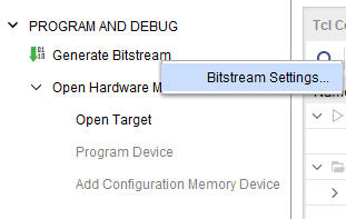
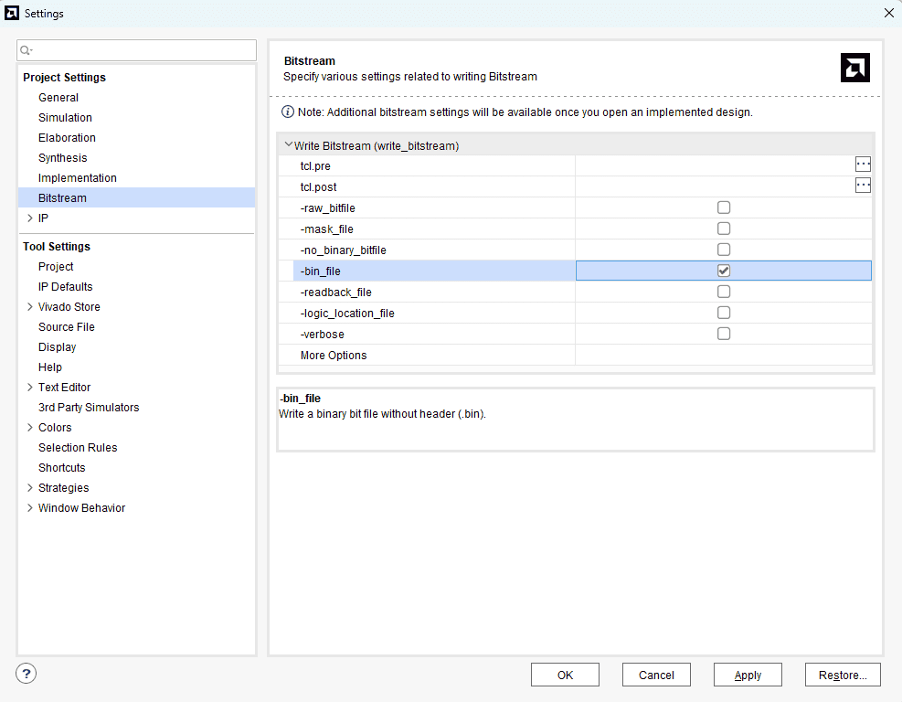
Step 1: It is recommended to generate a .bin bitstream file along with .bit bitstream file. Click “Bitstream Settings”.
Step 2: In the window that pops up, select the “-bin_file” option and click OK.
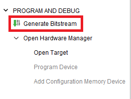
Step 3: Finally click “Generate Bitstream”.
Programming Mimas AU-Plus Using USB-JTAG
1. Ensure that switch SW2 (PGM SEL) is set to USB mode and Connect the USB Type-C cable to the FPGA board.
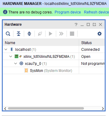
2. Click on “Auto connect” under hardware manager and it will automatically establish the connection.
Programming Mimas AU-Plus Using JTAG
Mimas AU-Plus Development Module features an onboard JTAG connector which facilitates easy reprogramming of SRAM and onboard SPI flash through JTAG programmer like “Xilinx Platform cable USB”. Following steps illustrate how to program FPGA on Mimas AU-Plus using JTAG.
Step 1: Ensure that switch SW2 is set to JTAG mode.
Step 2: By using JTAG cable, connect Xilinx platform cable USB to Mimas AU-Plus and power it up.
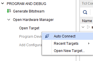
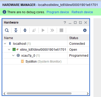
Step 3: Open Vivado project and open the target by clicking on the “Open Target” in “Open Hardware Manager” in the “Program and Debug” section of the Flow Navigator window. Select “Auto Connect”.
Step 4: If the device is detected successfully, then select “Program Device” after right clicking on the target device “XCAU7P_0” as shown below.
Step 5: In the dialog window which opens up, Vivado automatically chooses correct bitstream file if the design was synthesized, implemented and bitstream generated successfully. If needed, browse to the bitstream which needs to be programmed to FPGA. Finally, click “Program”.
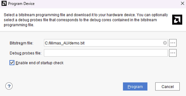
As soon as “Program” is clicked, a orange colored DONE LED (D1) on Mimas AU-Plus should light up, indicating that programming process is going on. This LED will turn off when the configuration is complete.
Programming QSPI Flash using Vivado
A .bin or .mcs file is required for programming Mimas AU-Plus onboard QSPI flash.
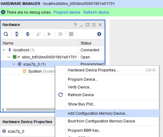
Step 1: Open Vivado project and open the target by clicking on the “Open Target” in “Open Hardware Manager” in the “Program and Debug” section of the Flow Navigator window. Select “Auto Connect”.
Step 2: If the device is detected successfully, then select “Add Configuration Memory Device” after right clicking on the target device “XCAU7P_0” as shown below.
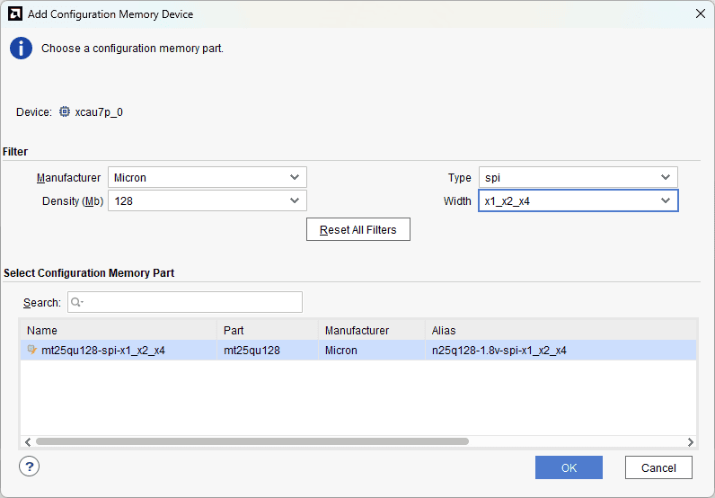
Step 3: Select the memory device “mt25ql128-spi-x1_x2_x4 (which is equivalent to n25q128-3.3v-spi-x1_x2_x4)”, then click OK.
Step 4: After completion of Step 3 the following dialog box will open. Click OK.
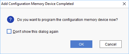
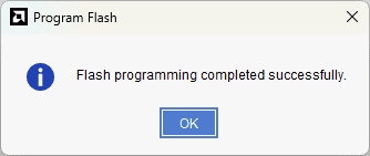
Step 5: Browse to the working .bin file or the .mcs file (whichever applicable) and click OK to program as shown below. If programming is successful, a confirmation message will be displayed.
Technical Specifications
| Parameter | Value | Unit |
|---|---|---|
| Basic Specifications | ||
| Number of PMODs | 2 | |
| On-board oscillator frequency (ASDMPLV-100.000MZ-LR-T3) | 100 | MHz |
| Quad SPI Flash Memory(MT25QU128ABA1ESE-0SIT TR) | 128 | Mb |
| DDR4(AS4C512M16DB-62BCN) | 8 | Gb |
| Syzygy connectors | 3 | |
| Power supply voltage (USB or External) | 5 | V |
| Operating Temperature | 0-70 | °C |
| Number of LEDs | 8 | |
| Number of Push Buttons | 4 | |
| Number of Dip Switches | 8 | |
| FPGA Specifications | ||
| Internal supply voltage relative to GND | -0.5 to 1.0 | V |
| Auxiliary supply voltage relative to GND | -0.5 to 2.0 | V |
| Output drivers supply voltage for HD I/O banks | –0.500 to 3.400 | V |
| Output drivers supply voltage for HP I/O banks and configuration bank 0 | –0.500 to 2.000 | V |
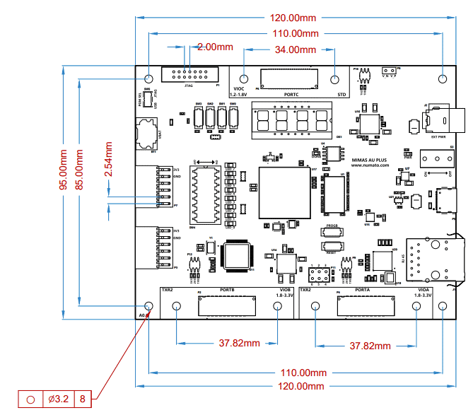
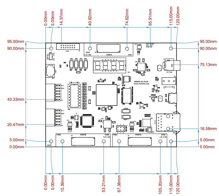
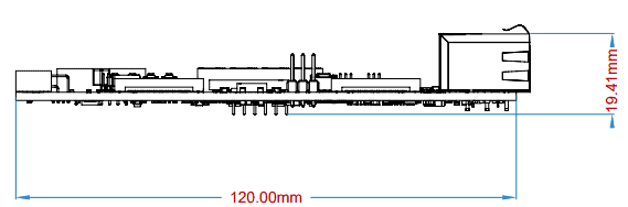
Mechanical Dimensions