Introduction
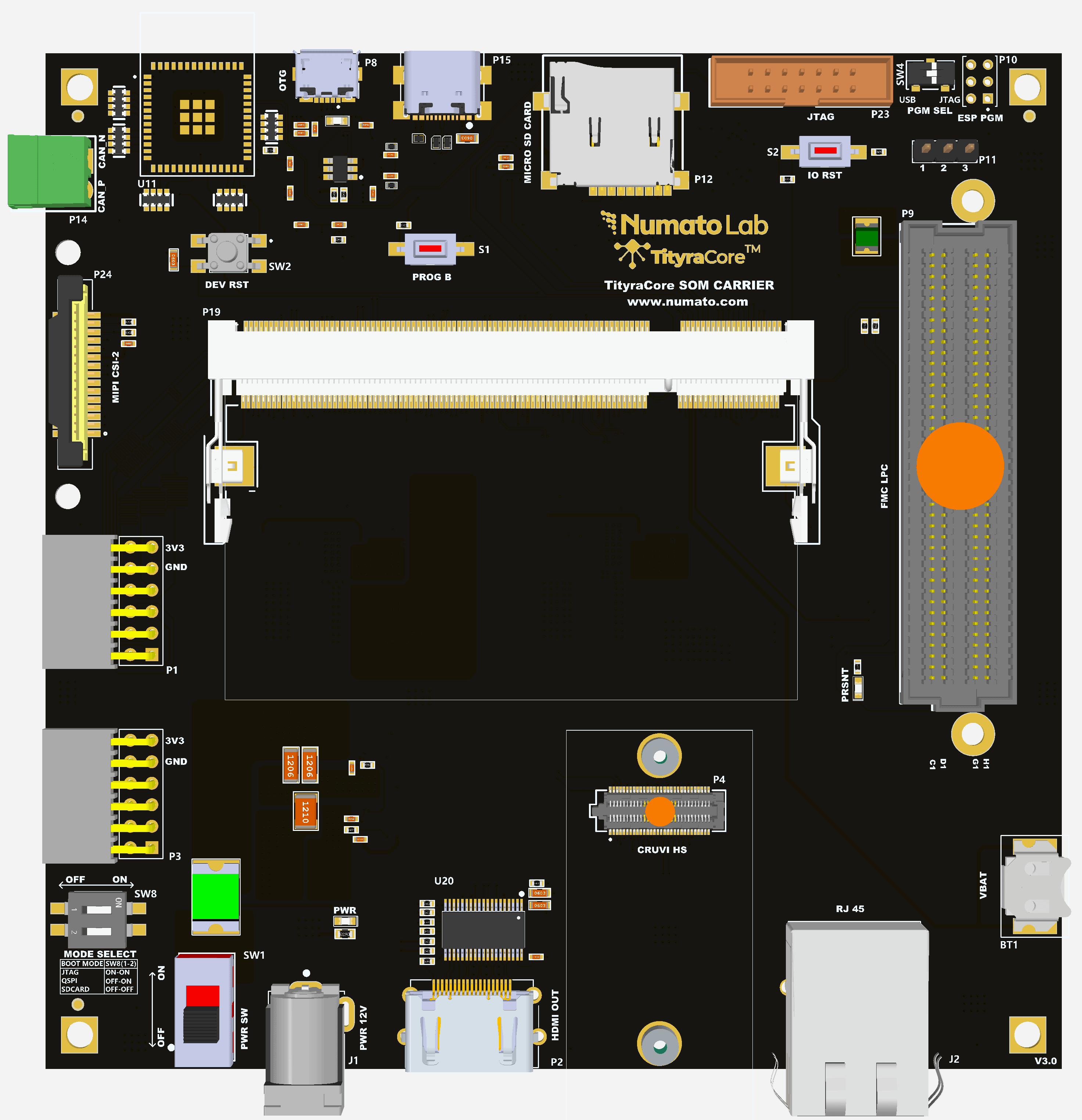
The TityraCore SoC Carrier enable the interfacing of various SODIMM modules, such as the TityraCore Z7 SoC SODIMM . The TityraCore SoC carrier includes a Low Pin Count (LPC) FMC connector, Gigabit ethernet connector, MicroSD Card slot and much more. Even though it has onboard peripherals, the number of peripherals can be increased using the 2×6 Header, CRUVI HS and FMC connectors.
Board Features
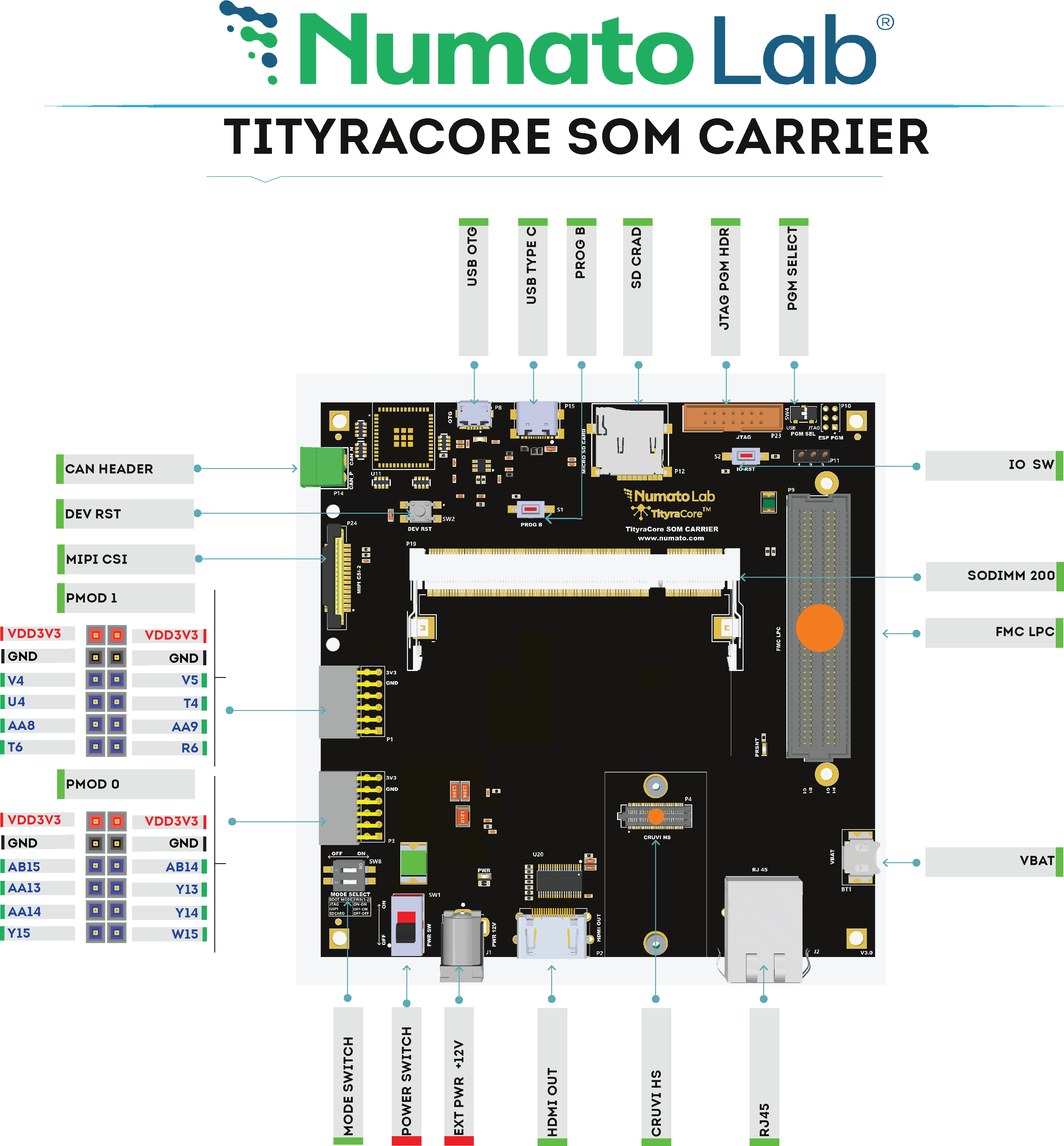
- SODIMM Connectors
- FTDI FT2232H for FPGA and Host communication
- RJ45 JACK
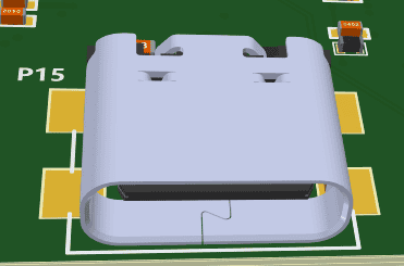
- USB Type-C connector
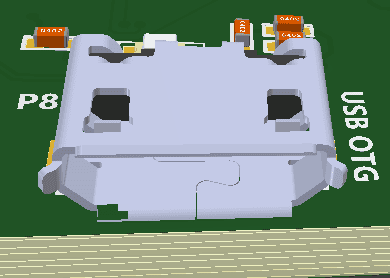
- USB micro-B connector for OTG communication
- 12V DC power supply
- JTAG Header for programming and debugging.
- FMC (LPC) connector with a maximum of 68 IOs for user-defined purpose
- Two 2×6 Expansion Header
- CAN Header
- microSD Card Slot
- MIPI camera interface
- ESP32 wi-fi module (reserved, installable on request)
- CRUVI HS connector
How to use TityraCore Carrier
The following sections describe how to use this module in detail. Detailed FPGA pin mappings are available in the TityraCore Z7 SoC SODIMM User Manual.
Hardware Accessories Required
In addition to the module, you may require the accessories listed below for a convenient and expedited installation:
- 12 V DC Power Supply.
- Micro-B cable.
- USB-C cable.
- AMD Platform Cable USB or compatible JTAG programmer.(optional)
- MicroSD card.
Connection Details
Reset Switch
The TityraCore SoC Carrier includes three reset mechanisms: a push-button switch labeled DEV RST connected to the FPGA’s system reset pin; PROG_B, which triggers reconfiguration of the FPGA; and IO RST, an active-high reset button used specifically for I/O configuration purposes.
Gigabit Ethernet port
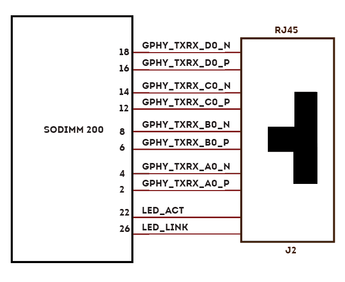
The TityraCore SoC Carrier features a 10/100/1000 Mbps Ethernet interface, with the FPGA pins directly connected to an RJ45 Ethernet jack. Additionally, it includes Activity and Link LEDs to provide status indicators for the user.
microSD Card Slot
TityraCore SoC Carrier supports a microSD card slot, offering additional non-volatile memory storage capacity.
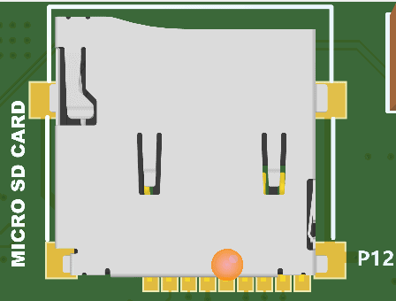
It operates in 3.3V and offers a compact and removable storage solution, making it ideal for storing data that exceeds the internal memory capacity of the FPGA. FPGAs can use microSD cards to store boot images or configuration data, which are loaded into the FPGA at startup.
Mode DIP Switches
TityraCore SoC Carrier has DIP switches (SW8) for changing the boot configuration of the FPGA based on the required functionality.
Boot Configuration:
The boot configuration of the TityraCore SoC will be based on the below configuration of switches:
SW8 1 2
JTAG ON ON
QSPI OFF ON
SD CARD OFF OFF
HDMI OUT
The onboard HDMI OUT interface makes the TityraCore SoC Carrier board an excellent platform for video rendering. The HDMI OUT interface is buffered using the HDMI buffer TPD12S520D BTR to ensure better signal strength and signal integrity.
| Pin No. | Signal Name | FPGA Pin Mapping |
|---|---|---|
| 1 | TX_CLK_P | B19 |
| 2 | TX_CLK_N | B20 |
| 3 | HDMI_TX0_P | G19 |
| 4 | HDMI_TX0_N | F19 |
| 5 | HDMI_TX1_P | E19 |
| 6 | HDMI_TX1_N | E20 |
| 7 | HDMI_TX2_P | G20 |
| 8 | HDMI_TX2_N | G21 |
| 9 | HDMI_TX_CEC | H22 |
| 10 | HDMI_TX_SCL | F21 |
| 11 | HDMI_TX_SDA | F22 |
| 12 | HDMI_TX_HOT | G22 |
PMOD
The TityraCore SoC Carrier features two 2×6 connectors, providing users with versatile options for interfacing with various peripherals and communication standards according to their application requirements
PMOD 0 PINS
| Pin No. | Signal name | FPGA pin Mapping |
|---|---|---|
| 1 | CONN0_D1 | W15 |
| 2 | CONN0_D2 | Y14 |
| 3 | CONN0_D3 | Y13 |
| 4 | CONN0_D4 | AB14 |
| 5 | GND | |
| 6 | VCC | |
| 7 | CONN0_D5 | Y15 |
| 8 | CONN0_D6 | AA14 |
| 9 | CONN0_D7 | AA13 |
| 10 | CONN0_D8 | AB15 |
| 11 | GND | |
| 12 | VCC |
PMOD 1 PINS
| Pin No. | Signal name | FPGA pin Mapping |
|---|---|---|
| 1 | CONN1_D1 | R6 |
| 2 | CONN1_D2 | AA9 |
| 3 | CONN1_D3 | T4 |
| 4 | CONN1_D4 | V5 |
| 5 | GND | |
| 6 | VCC | |
| 7 | CONN1_D5 | T6 |
| 8 | CONN1_D6 | AA8 |
| 9 | CONN1_D7 | U4 |
| 10 | CONN1_D8 | V4 |
| 11 | GND | |
| 12 | VCC |
CRUVI
TityraCore SoC Carrier supports CRUVI standard connectors for more complex applications. Customizable Ruggedized Universal VI is a universal connector for easy connection of peripheral modules to the main board, enabling developers to extend the functionality of their systems with minimal effort.
| Pin No. | Signal Name | FPGA pin Mapping |
|---|---|---|
| 1 | NC | NC |
| 2 | HSIO | C20 |
| 3 | NC | NC |
| 4 | VCC | VCC |
| 5 | SDA | AA4 |
| 6 | HSO | D20 |
| 7 | SCL | Y4 |
| 8 | HSRST | J22 |
| 9 | VCC | VCC |
| 10 | HSI | NC |
| 11 | REFCLK | NC |
| 12 | GND | GND |
| 13 | GND | GND |
| 14 | A0_P | P16 |
| 15 | B0_P | AB7 |
| 16 | A0_N | R16 |
| 17 | B0_N | AB6 |
| 18 | GND | GND |
| 19 | GND | GND |
| 20 | A1_P | J20 |
| 21 | B1_P | Y6 |
| 22 | A1_N | K21 |
| 23 | B1_N | Y5 |
| 24 | GND | GND |
| 25 | GND | GND |
| 26 | A2_P | R19 |
| 27 | B2_P | AA7 |
| 28 | A2_N | T19 |
| 29 | B2_N | AA6 |
| 30 | GND | GND |
| 31 | GND | GND |
| 32 | A3_P | R18 |
| 33 | B3_P | AB2 |
| 34 | A3_N | T18 |
| 35 | B3_N | AB1 |
| 36 | VADJ | VADJ |
| 37 | GND | GND |
| 38 | A4_P | K19 |
| 39 | B4_P | AB5 |
| 40 | A4_N | K20 |
| 41 | B4_N | AB4 |
| 42 | GND | GND |
| 43 | GND | GND |
| 44 | A5_P | L18 |
| 45 | B5_P | Y9 |
| 46 | A5_N | L19 |
| 47 | B5_N | Y8 |
| 48 | GND | GND |
| 49 | GND | GND |
| 50 | NC | NC |
| 51 | NC | NC |
| 52 | NC | NC |
| 53 | NC | NC |
| 54 | GND | GND |
| 55 | NC | NC |
| 56 | NC | NC |
| 57 | NC | NC |
| 58 | NC | NC |
| 59 | NC | NC |
| 60 | NC | NC |
RTC Cell Holder
The TityraCore SoC Carrier has a Coin Cell Holder (BT1) to support a 1.8V coin cell that will support 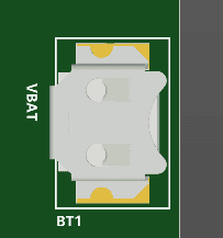
backup voltage for RTC when the main power supply is off. RTC maintains accurate timekeeping through these battery backups. The battery should be kept in the carrier board to provide voltage if the main power is off.
JTAG Header
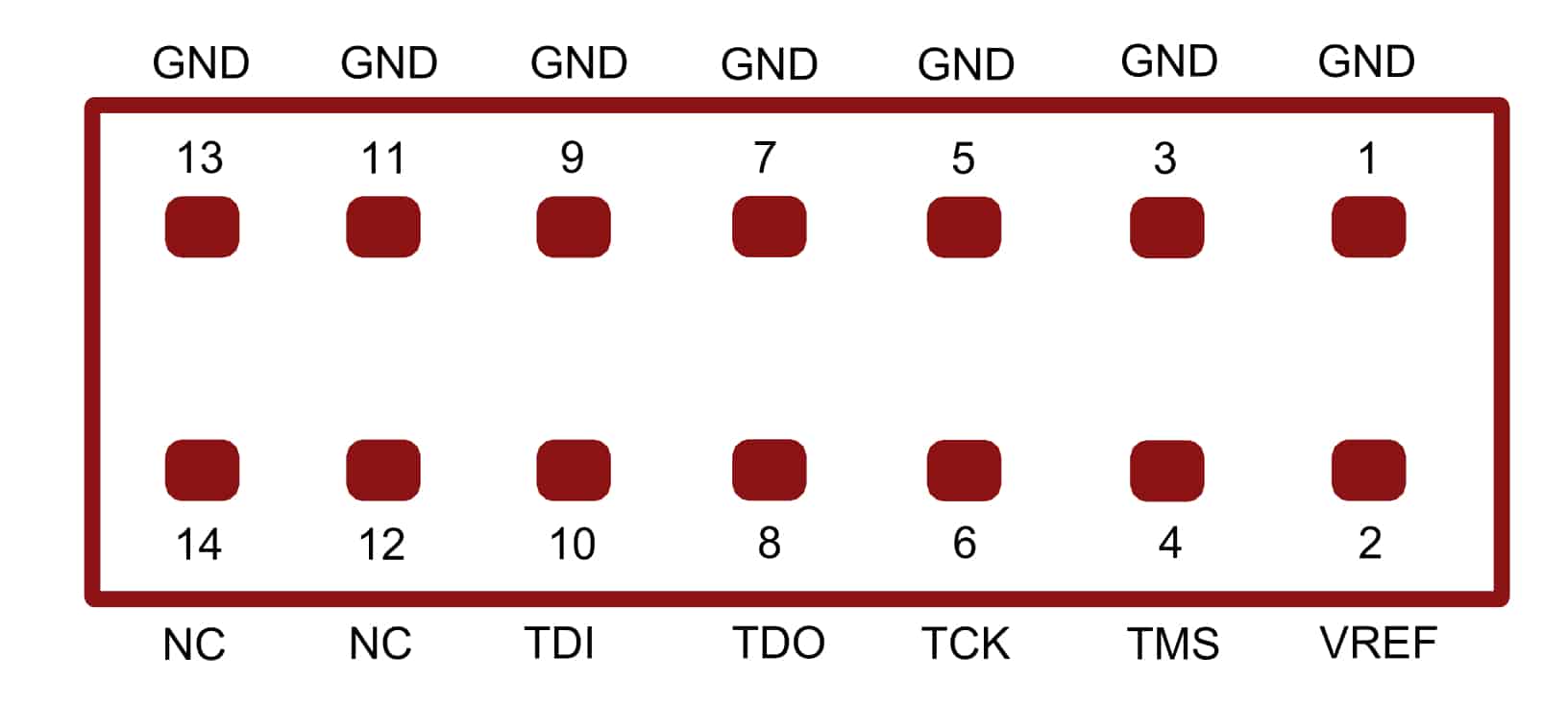
TityraCore SoC Carrier supports standard AMD 14-pin JTAG Header for debugging purposes.
JTAG (P23)
FMC Header
TityraCore features a low pin-count FMC connector which can be used to provide additional features and capabilities to it using custom or commercial-off-the-shelf daughter boards.
| C | FMC Pin Name | FPGA Pins | D | FMC Pin Name | FPGA Pins | G | FMC Pin Name | FPGA Pins | H | FMC Pin Name | FPGA Pins |
|---|---|---|---|---|---|---|---|---|---|---|---|
| C1 | GND | GND | D1 | PG_C2M | PG_C2M | G1 | GND | GND | H1 | NC | NC |
| C2 | NC | NC | D2 | GND | GND | G2 | NC | NC | H2 | PRSNT_M2C_L | PRSNT_M2C_L |
| C3 | NC | NC | D3 | GND | GND | G3 | NC | NC | H3 | GND | GND |
| C4 | GND | GND | D4 | NC | NC | G4 | GND | GND | H4 | NC | NC |
| C5 | GND | GND | D5 | NC | NC | G5 | GND | GND | H5 | NC | NC |
| C6 | NC | NC | D6 | GND | GND | G6 | FMC_LA00_CC_P | C17 | H6 | GND | GND |
| C7 | NC | NC | D7 | GND | GND | G7 | FMC_LA00_CC_N | C18 | H7 | FMC_LA02_P | F16 |
| C8 | GND | GND | D8 | FMC_LA01_CC_P | D18 | G8 | GND | GND | H8 | FMC_LA02_N | E16 |
| C9 | GND | GND | D9 | FMC_LA01_CC_N | C19 | G9 | FMC_LA03_P | D16 | H9 | GND | GND |
| C10 | FMC_LA06_P | F18 | D10 | GND | GND | G10 | FMC_LA03_N | D17 | H10 | FMC_LA04_P | E15 |
| C11 | FMC_LA06_N | E18 | D11 | FMC_LA05_P | G15 | G11 | GND | GND | H11 | FMC_LA04_N | D15 |
| C12 | GND | GND | D12 | FMC_LA05_N | G16 | G12 | FMC_LA08_P | C15 | H12 | GND | GND |
| C13 | GND | GND | D13 | GND | GND | G13 | FMC_LA08_N | B15 | H13 | FMC_LA07_P | G17 |
| C14 | FMC_LA10_P | A16 | D14 | FMC_LA09_P | B16 | G14 | GND | GND | H14 | FMC_LA07_N | F17 |
| C15 | FMC_LA10_N | A17 | D15 | FMC_LA09_N | B17 | G15 | FMC_LA12_P | A21 | H15 | GND | GND |
| C16 | GND | GND | D16 | GND | GND | G16 | FMC_LA12_N | A22 | H16 | FMC_LA11_P | A18 |
| C17 | GND | GND | D17 | FMC_LA13_P | D22 | G17 | GND | GND | H17 | FMC_LA11_N | A19 |
| C18 | FMC_LA14_P | E21 | D18 | FMC_LA13_N | C22 | G18 | FMC_LA16_P | H19 | H18 | GND | GND |
| C19 | FMC_LA14_N | D21 | D19 | GND | GND | G19 | FMC_LA16_N | H20 | H19 | FMC_LA15_P | B21 |
| C20 | GND | GND | D20 | FMC_LA17_CC_P | Y19 | G20 | GND | GND | H20 | FMC_LA15_N | B22 |
| C21 | GND | GND | D21 | FMC_LA17_CC_N | AA19 | G21 | FMC_LA20_P | T22 | H21 | GND | GND |
| C22 | FMC_LA18_CC_P | Y18 | D22 | GND | GND | G22 | FMC_LA20_N | U22 | H22 | FMC_LA19_P | T21 |
| C23 | FMC_LA18_CC_N | AA18 | D23 | FMC_LA23_P | U20 | G23 | GND | GND | H23 | FMC_LA19_N | U21 |
| C24 | GND | GND | D24 | FMC_LA23_N | V20 | G24 | FMC_LA22_P | W20 | H24 | GND | GND |
| C25 | GND | GND | D25 | GND | GND | G25 | FMC_LA22_N | W21 | H25 | FMC_LA21_P | V22 |
| C26 | FMC_LA27_P | Y20 | D26 | FMC_LA26_P | AA21 | G26 | GND | GND | H26 | FMC_LA21_N | W22 |
| C27 | FMC_LA27_N | Y21 | D27 | FMC_LA26_N | AB21 | G27 | FMC_LA25_P | AA22 | H27 | GND | GND |
| C28 | GND | GND | D28 | GND | GND | G28 | FMC_LA25_N | AB22 | H28 | FMC_LA24_P | V18 |
| C29 | GND | GND | D29 | NC | NC | G29 | GND | GND | H29 | FMC_LA24_N | V9 |
| C30 | NC | NC | D30 | NC | NC | G30 | FMC_LA29_P | U17 | H30 | GND | GND |
| C31 | NC | NC | D31 | NC | NC | G31 | FMC_LA29_N | V17 | H31 | FMC_LA28_P | AB19 |
| C32 | GND | GND | D32 | 3V3AUX | 3V3AUX | G32 | GND | GND | H32 | FMC_LA28_N | AB20 |
| C33 | GND | GND | D33 | NC | NC | G33 | FMC_LA31_P | AA16 | H33 | GND | GND |
| C34 | GND | GND | D34 | NC | NC | G34 | FMC_LA31_N | AB16 | H34 | FMC_LA30_P | AA17 |
| C35 | P12V0 | P12V0 | D35 | P3V3 | P3V3 | G35 | GND | GND | H35 | FMC_LA30_N | AB17 |
| C36 | GND | GND | D36 | P3V3 | P3V3 | G36 | FMC_LA33_P | V13 | H36 | GND | GND |
| C37 | P12V0 | P12V0 | D37 | GND | GND | G37 | FMC_LA33_N | W13 | H37 | FMC_LA32_P | V14 |
| C38 | GND | P12V0 | D38 | P3V3 | P3V3 | G38 | GND | GND | H38 | FMC_LA32_N | V15 |
| C39 | P3V3 | P3V3 | D39 | GND | GND | G39 | VADJ | VADJ | H39 | GND | GND |
| C40 | GND | GND | D40 | P3V3 | P3V3 | G40 | GND | GND | H40 | VADJ | VADJ |
SODIMM Connector
| Signal Name | SODIMM Pin(Top) | SODIMM Pin(Bottom) | Signal Name |
|---|---|---|---|
| GND | 1 | 2 | GPHY_TXRX_A0_P |
| DEV_RST | 3 | 4 | GPHY_TXRX_A0_N |
| GND | 5 | 6 | GPHY_TXRX_B0_P |
| MIPI_L0_P | 7 | 8 | GPHY_TXRX_B0_N |
| MIPI_L0_N | 9 | 10 | GND |
| MIPI_L1_P | 11 | 12 | GPHY_TXRX_C0_P |
| MIPI_L1_N | 13 | 14 | GPHY_TXRX_C0_N |
| MIPI_CLK_P | 15 | 16 | GPHY_TXRX_D0_P |
| MIPI_CLK_N | 17 | 18 | GPHY_TXRX_D0_N |
| CAM_GPIO | 19 | 20 | GND |
| CAM_CLK | 21 | 22 | LED0/Activity |
| CAM_SCL | 23 | 24 | VCC3V3 |
| CAM_SDA | 25 | 26 | LED0/Link |
| GND | 27 | 28 | MODE_0 |
| FPGA_TDI | 29 | 30 | MODE_1 |
| FPGA_TDO | 31 | 32 | VCC3V3 |
| FPGA_TMS | 33 | 34 | PG_ALL |
| FPGA_TCK | 35 | 36 | VBAT |
| UART_TX | 37 | 38 | PROG_B |
| UART_RX | 39 | 40 | GND |
| GND | 41 | 42 | CAN_TX |
| FPGA_SCK | 43 | 44 | CAN_RX |
| FPGA_MOSI | 45 | 46 | VCC3V3 |
| GND | 47 | 48 | FMC_LA11_P |
| FPGA_MISO | 49 | 50 | FMC_LA11_N |
| SD_DATA1 | 51 | 52 | FMC_LA09_P |
| SD_DATA2 | 53 | 54 | FMC_LA09_N |
| FPGA_SS | 55 | 56 | FMC_LA10_P |
| IO_RESET | 57 | 58 | FMC_LA10_N |
| HSRST | 59 | 60 | VCC3V3 |
| FMC_LA00_CC_P | 61 | 62 | FMC_LA08_P |
| FMC_LA00_CC_N | 63 | 64 | FMC_LA08_N |
| GND | 65 | 66 | FMC_LA02_P |
| SCL | 67 | 68 | FMC_LA02_N |
| SDA | 69 | 70 | B4_P |
| B1_P | 71 | 72 | VCC3V3 |
| B1_N | 73 | 74 | B4_N |
| B2_P | 75 | 76 | FMC_LA07_P |
| B2_N | 77 | 78 | FMC_LA07_N |
| GND | 79 | 80 | FMC_LA06_P |
| FMC_LA14_P | 81 | 82 | FMC_LA06_N |
| FMC_LA14_N | 83 | 84 | CONN1_D2 |
| HDMI_TX_CEC | 85 | 86 | CONN1_D6 |
| HDMI_TX_HOT | 87 | 88 | VCC3V3 |
| B5_P | 89 | 90 | HDMI_TX_SCL |
| B5_N | 91 | 92 | HDMI_TX_SCA |
| B0_P | 93 | 94 | FMC_LA13_P |
| GND | 95 | 96 | FMC_LA13_N |
| B0_N | 97 | 98 | B3_P |
| HSO | 99 | 100 | B3_N |
| HSIO | 101 | 102 | FMC_LA15_P |
| FMC_LA12_P | 103 | 104 | FMC_LA15_N |
| FMC_LA12_N | 105 | 106 | VCC3V3 |
| CONN1_D1 | 107 | 108 | CONN1_D4 |
| CONN1_D5 | 109 | 110 | CONN1_D8 |
| CONN1_D3 | 111 | 112 | FMC_LA03_P |
| GND | 113 | 114 | FMC_LA03_N |
| CONN1_D7 | 115 | 116 | HDMI_TX_CLK_P |
| FMC_LA01_CC_P | 117 | 118 | HDMI_TX_CLK_N |
| FMC_LA01_CC_N | 119 | 120 | FMC_LA05_P |
| FMC_LA04_P | 121 | 122 | FMC_LA05_N |
| FMC_LA04_N | 123 | 124 | VCC3V3 |
| HDMI_TX2_P | 125 | 126 | FMC_LA16_P |
| HDMI_TX2_N | 127 | 128 | FMC_LA16_N |
| HDMI_TX0_P | 129 | 130 | HDMI_TX1_P |
| GND | 131 | 132 | HDMI_TX1_N |
| HDMI_TX0_N | 133 | 134 | CONN0_D4 |
| CONN0_D3 | 135 | 136 | CONN0_D8 |
| CONN0_D7 | 137 | 138 | A0_P |
| CONN0_D2 | 139 | 140 | A0_N |
| CONN0_D6 | 141 | 142 | VCC3V3 |
| FMC_LA22_P | 143 | 144 | A1_P |
| FMC_LA22_N | 145 | 146 | A1_N |
| FMC_LA21_P | 147 | 148 | FMC_LA19_P |
| FMC_LA21_N | 149 | 150 | FMC_LA19_N |
| GND | 151 | 152 | A2_P |
| FMC_LA20_P | 153 | 154 | A2_N |
| FMC_LA20_N | 155 | 156 | A3_P |
| A5_P | 157 | 158 | A3_N |
| A5_N | 159 | 160 | VCC3V3 |
| FMC_LA32_P | 161 | 162 | A4_P |
| FMC_LA32_N | 163 | 164 | A4_N |
| FMC_LA29_P | 165 | 166 | FMC_LA31_P |
| FMC_LA29_N | 167 | 168 | FMC_LA31_N |
| GND | 169 | 170 | FMC_LA33_P |
| FMC_LA30_P | 171 | 172 | FMC_LA33_N |
| FMC_LA30_N | 173 | 174 | CONN0_D1 |
| FMC_LA18_CC_P | 175 | 176 | CONN0_D5 |
| FMC_LA18_CC_N | 177 | 178 | FMC_LA28_P |
| FMC_LA17_CC_P | 179 | 180 | VCC3V3 |
| FMC_LA17_CC_N | 181 | 182 | FMC_LA28_N |
| FMC_LA25_P | 183 | 184 | FMC_LA28_P |
| GND | 185 | 186 | GND |
| FMC_LA25_N | 187 | 188 | FMC_LA26_N |
| FMC_LA27_P | 189 | 190 | OTG_USB_ID |
| FMC_LA27_N | 191 | 192 | OTG_USB_5V |
| FMC_LA23_P | 193 | 194 | OTG_D_P |
| FMC_LA23_N | 195 | 196 | OTG_D_N |
| FMC_LA24_P | 197 | 198 | GND |
| FMC_LA24_N | 199 | 200 | 5V0 |
Technical Specifications
| Parameter | value | Unit |
|---|---|---|
| Basic Specification | ||
| Power supply voltage | 12 | V |
| Number of pins | 200 | |
| Height above the board | 5.20 | mm |
| Pitch | 0.60 | mm |
| Temperature | 0-70 | °C |
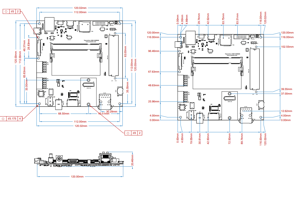
Mechanical Dimensions
