1.Introduction
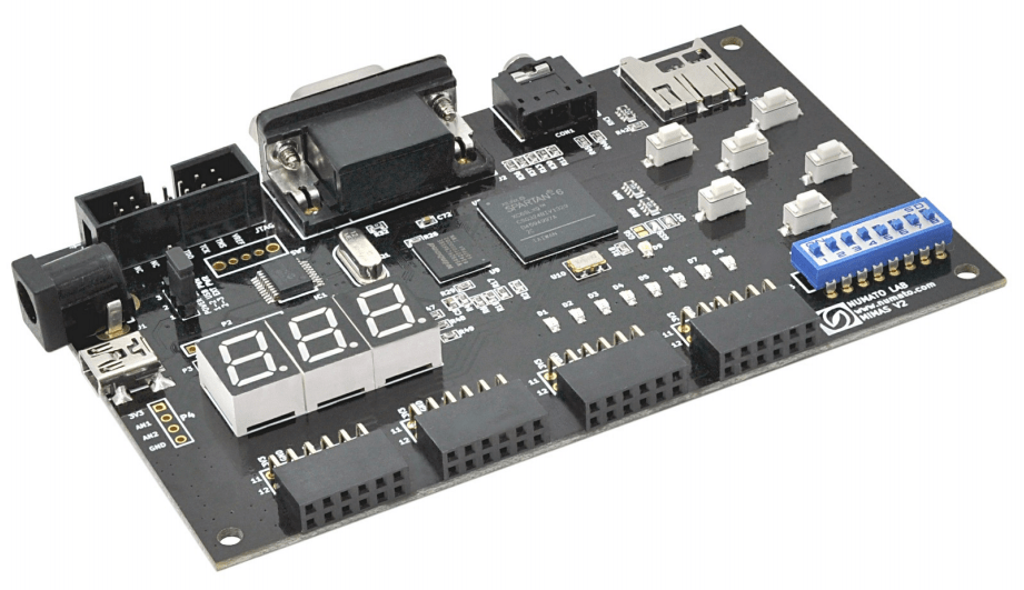
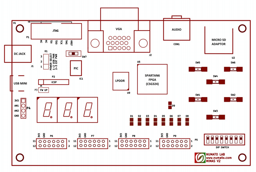
MIMAS V2 is a feature-packed yet low-cost FPGA Development board featuring Xilinx Spartan-6 FPGA. It is specially designed for experimenting and learning system design with FPGAs. This development board features SPARTAN XC6SLX9 CSG324 FPGA with onboard 512Mb DDR SDRAM. The USB 2.0 interface provides fast and easy configuration download to the on-board SPI flash. No need to buy an expensive programmer or special downloader cable to download the bitstream to the board.
Applications
- Product Prototype Development
- Signal Processing
- Learning Digital Electronics
- Educational tool for schools and universities
Board features
- FPGA: Spartan XC6SLX9 in CSG324 package
- DDR: 166MHz 512Mb LPDDR (MT46H32M16LF/W949D6CBHX6E)
- Flash memory: 16 Mb SPI flash memory (M25P16)
- USB 2.0 interface for On-board flash programming
- FPGA configuration via JTAG and USB
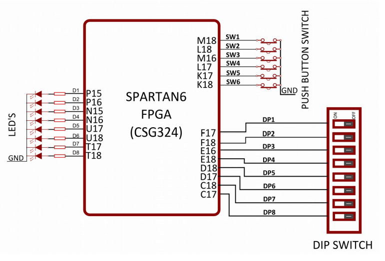
- 8 LEDs Six Push Buttons and 8 way DIP switch for user-defined purposes
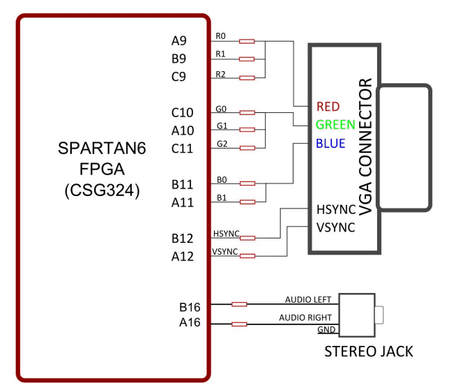
- VGA Connector
- Stereo Jack
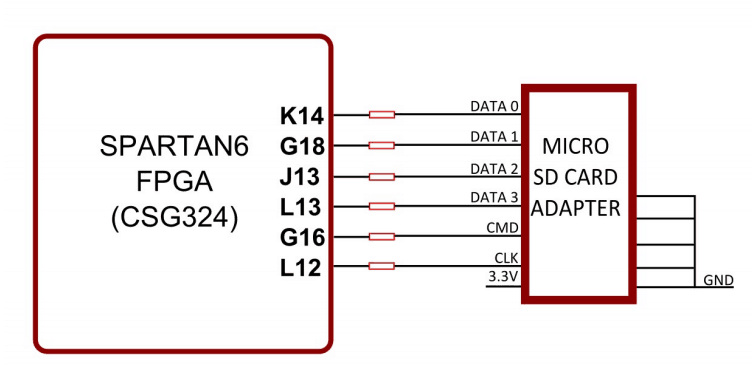
- Micro SD Card Adapter
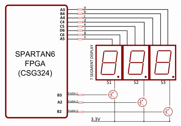
- Three-Digit Seven Segment Display.
- 32 IOs for user-defined purposes
- Four 6×2 Expansion Connectors
- On-board voltage regulators for single power rail operation
2.How to Use Mimas V2 Spartan 6 FPGA Development Board
2.1.Components/Tools Required
Along with the module, you may need the items in the list below for easy and fast installation.
1. USB A to Mini B cable.
2. DC Power supply (Optional).
2.2.Connection Diagram
This diagram should be used as a reference only. For detailed information, see MIMAS V2 schematics at the end of this documentation. The details of individual connectors are as below.
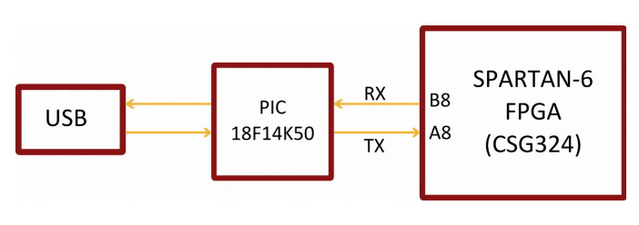
2.3.USB Interface
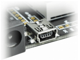 The onboard full-speed USB controller helps a computer to communicate with this module. Use a USB A to Mini B cable to connect with a PC. By default, the module is powered from USB so make sure not to overcrowd unpowered USB hubs.
2.4.DC Power Supply
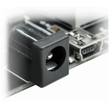 This module uses a +5V power supply to function properly. By default, the board is configured to use the +5V supply from USB. So an external +5V power is not required unless the USB port is unable to supply enough current. In most cases, USB ports are capable of providing enough current for the module. The current requirement for this board largely depends on your application. Please consult the FPGA datasheet for more details on power requirements. If for any reason, an external 5V power supply needs to be used for the module, the Power select jumper should be configured properly before connecting the power supply. Please refer to the marking on the board for more details.
2.5.Power Select
The Power Select header K1 is used to configure the power source for the board. The jumper in pin 1 and 2 is shorted to switch the power source to the onboard USB port and pin 2 and 3 to use the external DC power.
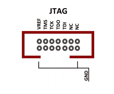
2.6.JTAG Connector
A JTAG connector provides access to FPGA’s JTAG pins. A XILINX platform cable can be used for JTAG programming.
2.7.Configuration Mode Selection
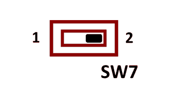
Slide switch SW7 is used to switch between the USB configuration mode and UART. Slide the switch to Position 1 to download bitstream through USB configuration tool and Position 2 to use the interface as a UART in order to communicate from your code in FPGA with the PC. By default, the board is shipped with a slide switch position in the USB configuration tool mode.
2.8.UART
The MIMAS V2 includes USB-UART, which helps to establish the communication between the code in the FPGA and any application running on the PC. Data can be sent and received from the FPGA by using Serial Terminal at baud rate 19200.
2.9.LED, Push Button and Dip Switch
MIMAS V2 has six push-button switches, an eight-position DIP switch and eight LEDs for human interaction. All switches are directly connected to Spartan 6 FPGA and can be used in your design with minimal effort.
2.10.Micro SD
MIMAS V2 features a Micro SD adapter on-board. By installing a Micro SD card, you can add data logging, media storage and other file storage to your design.
2.11.VGA and Audio
The VGA interface provides this board the ability to generate VGA signals from FPGA and display information on any Display/monitor that supports standard VGA connector. This VGA interface uses resistor network-based DAC for easy code implementation. This 8 bit VGA interface can display up to 256 colors.
Two IOs on the FPGA is dedicated to generating two channels of audio. Different audio tones can be generated by using PWM and Frequency synthesis.
2.12.7Segment LED Display
This board features three 7-segment LED display multiplexed for low pin count operation. Each module can be separately turned on and off with the three switching transistors.
Note: All signals (a, b, c, d, e, f, g, dot, enable 1, enable 2, enable 3) used for controlling 7-Segment display are active-low signals. So, for example, for displaying “8” in display-2, users need to drive Enable 2 to 0 as well as drive signals a, b, c, d, e, f to 0. All other signals need to be driven to 1.
2.13.GPIOs
This board is equipped with 32 user IO pins that can be used for various custom applications. Pin assignments on the connectors are available in the tables below.
HEADER P6
| Header Pin No. | Pin description | Spartan-6 (CSG324) Pin No. |
|---|---|---|
| 1 | IO_L43P_2 | U7 |
| 2 | IO_L43N_2 | V7 |
| 3 | IO_L63P_2 | T4 |
| 4 | IO_L63N_2 | V4 |
| 5 | IO_L49P_D3_2 | U5 |
| 6 | IO_L49N_D4_2 | V5 |
| 7 | IO_L62P_D5_2 | R3 |
| 8 | IO_L62N_D6_2 | T3 |
| 9 | GND | NA |
| 10 | GND | NA |
| 11 | VCCAUX | NA |
| 12 | VCCAUX | NA |
HEADER P7
| Header Pin No. | Pin description | Spartan-6 (CSG324) Pin No. |
|---|---|---|
| 1 | IO_L41P_2 | U8 |
| 2 | IO_L41N_VREF_2 | V8 |
| 3 | IO_L31P_GCLK31_D14_2 | R8 |
| 4 | IO_L31N_GCLK30_D15_2 | T8 |
| 5 | IO_L48P_D7_2 | R5 |
| 6 | IO_L48N_RDWR_B_VREF_2 | T5 |
| 7 | IO_L32P_GCLK29_2 | T9 |
| 8 | IO_L32N_GCLK28_2 | V9 |
| 9 | GND | NA |
| 10 | GND | NA |
| 11 | VCCAUX | NA |
| 12 | VCCAUX | NA |
HEADER P8
| Header Pin No. | Pin description | Spartan-6 (CSG324) Pin No. |
|---|---|---|
| 1 | IO_L16P_2 | R11 |
| 2 | IO_L16N_VREF_2 | T11 |
| 3 | IO_L29P_GCLK3_2 | R10 |
| 4 | IO_L29N_GCLK2_2 | T10 |
| 5 | IO_L14P_D11_2 | U13 |
| 6 | IO_L14N_D12_2 | V13 |
| 7 | IO_L23P_2 | U11 |
| 8 | IO_L23N_2 | V11 |
| 9 | GND | NA |
| 10 | GND | NA |
| 11 | VCCAUX | NA |
| 12 | VCCAUX | NA |
HEADER P9
| Header Pin No. | Pin description | Spartan-6 (CSG324) Pin No. |
|---|---|---|
| 1 | IO_L43P_GCLK5_M1DQ4_1 | H17 |
| 2 | IO_L43N_GCLK4_M1DQ5_1 | H18 |
| 3 | IO_L44P_A3_M1DQ6_1 | J16 |
| 4 | IO_L44N_A2_M1DQ7_1 | J18 |
| 5 | IO_L41P_GCLK9_IRDY1_M1RASN_1 | K15 |
| 6 | IO_L41N_GCLK8_M1CASN_1 | K16 |
| 7 | IO_L42P_GCLK7_M1UDM_1 | L15 |
| 8 | IO_L42N_GCLK6_TRDY1_M1LDM_1 | L16 |
| 9 | GND | NA |
| 10 | GND | NA |
| 11 | VCCAUX | NA |
| 12 | VCCAUX | NA |
3.Driver Installation
3.1.Installing on Windows
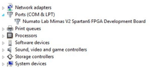 This product requires a driver to be installed for proper functioning when used with Windows. The driver package can be downloaded from the product page. To install the driver, unzip the contents of the downloaded driver package to a folder. Attach the USB cable to the PC and when asked by Windows device installation wizard, point to the folder where driver files are present. When the driver installation is complete, the module should appear in Windows Device Manager as a serial port (see the picture on the right). Note down the name of the serial port (COM1, COM2, etc..). This information is required while programming the module with the configuration tool.
3.2.Installing on Linux
To use this product with Linux, the USB CDC driver needs to be compiled in with the kernel. Fortunately, most Linux distributions (Ubuntu, Redhat, Debian, etc..) have this driver pre-installed. The chances of you requiring to rebuild the kernel to include the USB CDC driver is very slim. When connected to a Linux machine, this product should appear as a serial port in the /dev directory. Usually, the name of the device will be “ttyACMx” or similar. The name may be different depending on the Linux distribution you have.
3.3.Installing on Mac
Similar to Linux, Mac operating system comes with the required drivers pre-installed. When connected to a Mac computer, the device should appear as a serial port.
4.Generating Bit Stream for MIMAS V2
HDL design needs to be converted to a bit stream before it can be programmed to FPGA. MIMAS V2 configuration tool at this time accepts only binary (.bin) bitstream created by XILINX ISE (http://www.xilinx.com/tools/webpack.htm). Once the HDL is synthesized, it is easy to create a binary bitstream out of it. Please follow the steps below to generate a binary bitstream from your design using ISE Web Pack.
Step 1: Right-click on the “Generate Programming File” option in the “Processes” window.
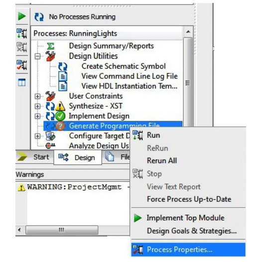
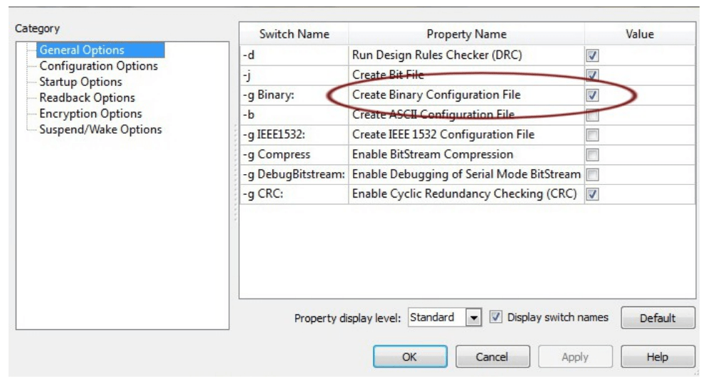
Step 2: Select “Process Properties” from the pop-up menu. In the dialog box, check the “Create Binary Configuration File” Checkbox and click “Apply”.
Step 3: Click “OK” to close the dialog box. Right-click on the “Generate Programming File” option again and select “Run”. Now you will be able to find a .bin file in the project directory and that file can be used for MIMAS V2 configuration.
5.Powering Up MIMAS V2
MIMAS V2 can be powered directly from the USB port so make sure that you are using a USB port that can power the board properly. It is recommended to connect the board directly to the PC instead of using a hub. It is practically very difficult to estimate the power consumption of the board, as it depends heavily on your design and the clock used. XILINX provides tools to estimate power consumption. In any case, if power from USB is not enough for your application, an external supply can be applied to the board. MIMAS V2 requires two different voltages, a 3.3V, and a 1.2V supply. On-board regulators derive these voltages from the USB/Ext power supply
6.Configuring MIMAS V2
The MIMAS V2 Spartan6 module can be configured by two methods,
a) Using the MIMAS V2 configuration tool through USB.
b) Using the Xilinx programming cable.
6.1.Configuring MIMAS V2 Using Configuration Tool
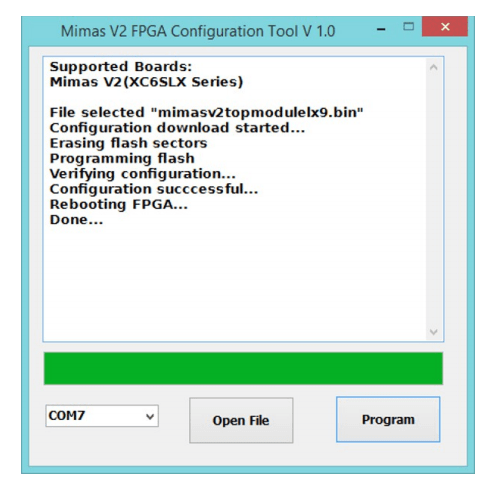
MIMAS V2 has an on-board micro-controller which facilitates easy reprogramming of onboard SPI flash through the USB interface. The micro-controller receives bitstream from the host application and program it into the SPI Flash and lets the FPGA boot from the flash. The MIMAS V2 configuration application can be downloaded from www.numato.com for free. When MIMAS V2 is connected to PC, it shows up as a COM port in Device Manager. Run configuration application, select correct COM Port before downloading bitstream. Click on “Open File” to select the bitstream file (.bin) and press the “Program” button to download the bitstream. Wait till the download process is finished. Once the download process is over, the configuration controller will try to boot the FPGA from the SPI Flash automatically. Follow the below steps.
Step 1: Make sure you have selected USB configuration mode (Slide SW7 to position 1. Refer to the section “Configuration Mode Selection” for more information). Run MIMAS V2 Configuration Tool and select the correct port (Refer to section “Driver installation” for more information on finding the port number). Click the Open file button and select the .bin file.
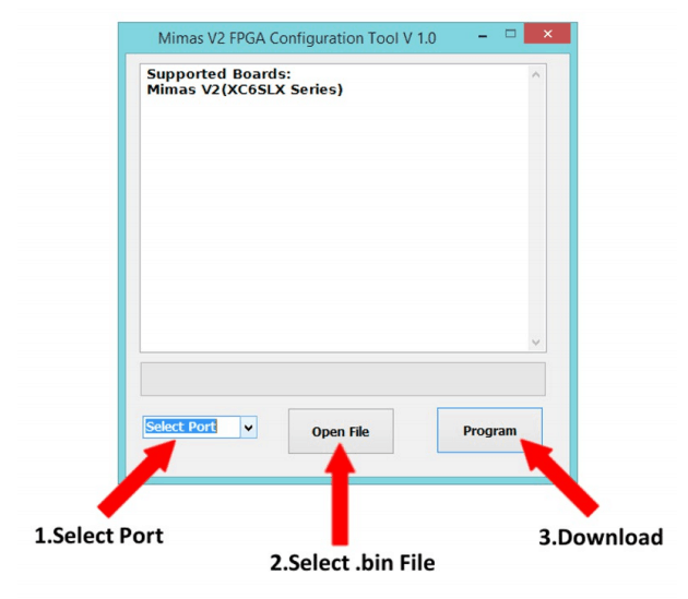
Step 2: Click on the “Program” button. Wait till “Done” appears on the screen.
6.2.Configuring MIMAS V2 Using JTAG
MIMAS V2 Spartan6 module features an onboard JTAG connector that facilitates easy reprogramming of SRAM and onboard SPI flash through JTAG programmer like “XILINX Platform-cable usb”. Programming MIMAS V2 using JTAG requires “XILINX ISE iMPACT” software which is bundled with XILINX ISE Design Suite. To program SPI flash we need a “.mcs” file that needs to be generated from the “.bit” file. Steps for generating the “.mcs” file are discussed below. Programming FPGA SRAM does not require a .mcs file to be generated.
Generating “.mcs” file for MIMAS V2
Step 1: Open ISE iMPACT. Click on “Create PROM file(PROM file formatter)”.In the dialog box, select “Configure Single FPGA” in the storage device type. Then click on the green arrow on the right side.
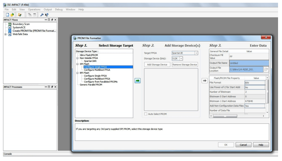
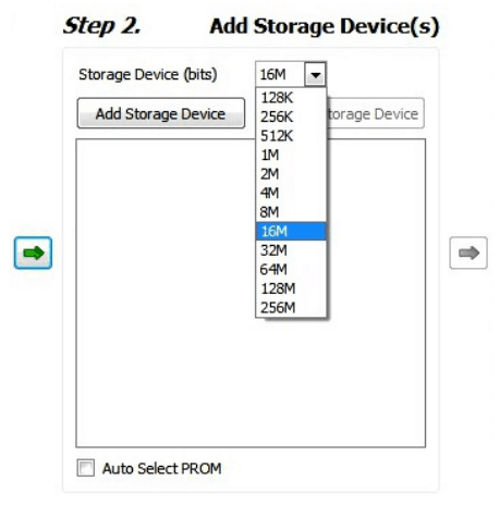
Step 2: Select the 16M in Storage Device (bits) list. Now click on “Add Storage Device”, then the green arrow at the right side.
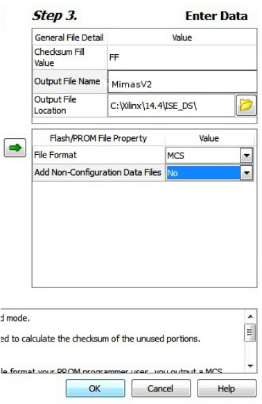
Step 3: Set an output file name and an output file location (the “.mcs” file will be generated at this location which will be required later for programming the FPGA), then click OK twice, then select the “.bit” file we already generated then click Open and click NO when it prompts to add another device file.
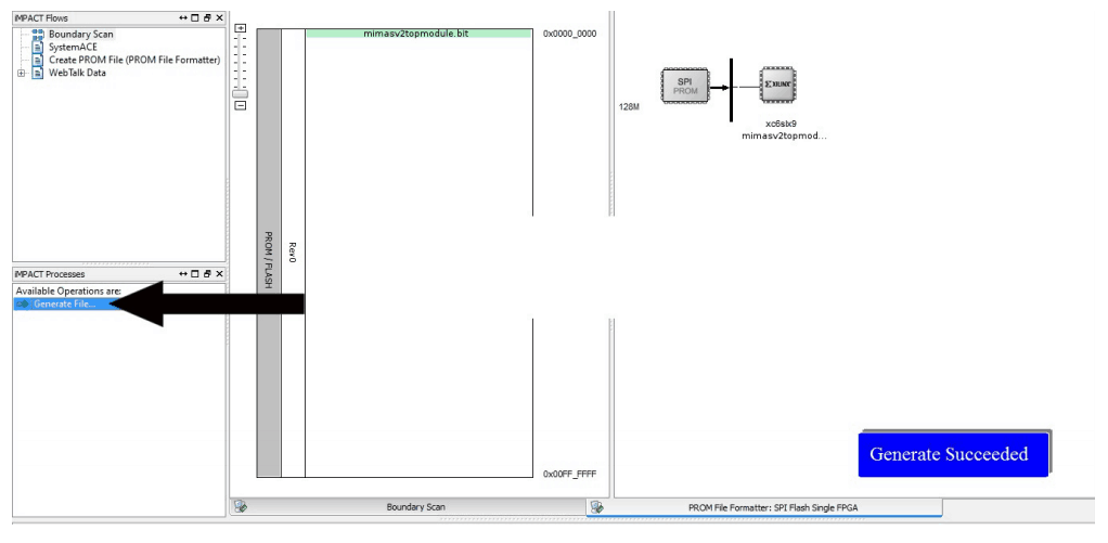
Step 4: Double click on “Generate File”. A message “Generate Succeeded” will be displayed as shown in fig below if the .mcs file is generated successfully.
6.3.Programming Onboard SPI flash Using ISE iMPACT
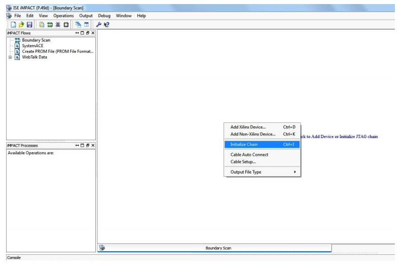
Step 1: Make sure the Xilinx Platform Cable USB is connected properly to the board. Open ISE iMPACT. Click on “Boundary Scan” in the iMPACT flows window in the left top corner. Then right-click on the window panel on the right side. Select “Initialize Chain”.
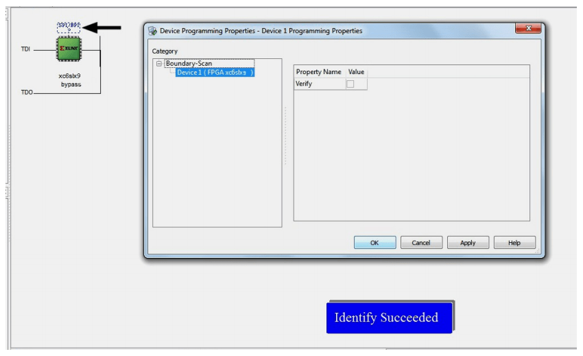
Step 2: If the device is detected properly you will get a pop-up window as shown below, Click OK. Then right-click on the SPI/BPI (next to the black arrow in the below fig.), select Add SPI/BPI Flash.
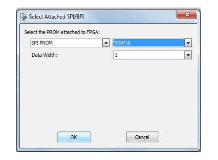
Step 3: Select the “.mcs” file we already created and click OK. Now choose “M25P16” in the dialogue box appeared, then click OK.
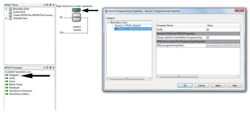
Step 4: Click on “Flash”, Double Click on Program, select OK. If the programming is successful, a confirmation message will be displayed.
7.Technical Specifications
| Parameter * | Value | Unit |
|---|---|---|
| Basic Specifications | ||
| Number of GPIOs | 32 | |
| Number of LEDs | 8 | |
| Number of Push Buttons | 6 | |
| SPI Flash Memory (M25P16) | 16 | Mb |
| Power supply voltage (USB or external) | 5 - 7 | V |
| FPGA Specifications | ||
| Internal supply voltage relative to GND | –0.5 to 1.25 | V |
| Auxiliary supply voltage relative to GND | –0.5 to 3.75 | V |
| Output drivers supply voltage relative to GND | –0.5 to 3.75 | V |
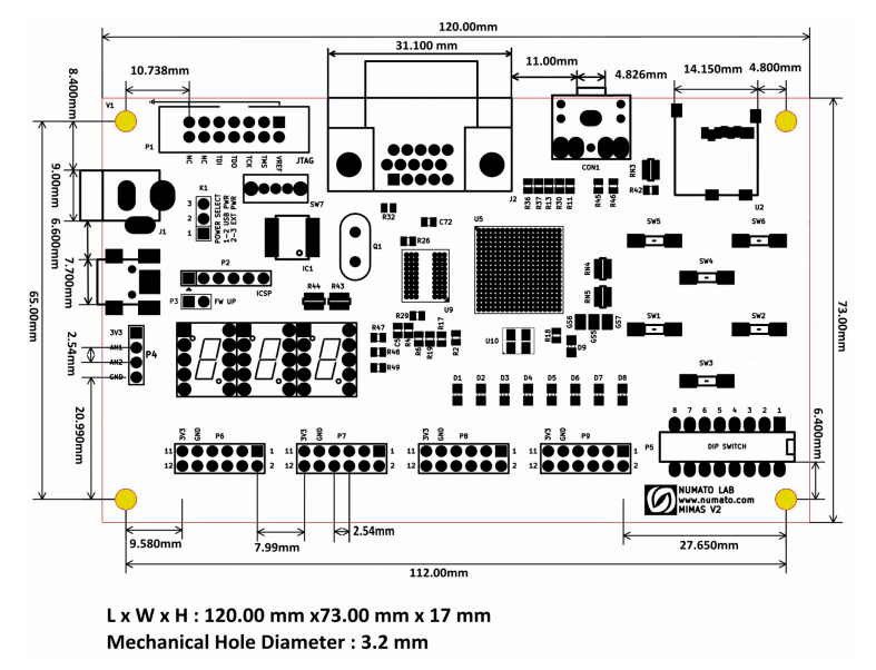
8.Mechanical Dimensions