Introduction
Introducing the Elbert S7 FPGA Development Board: Unleash your creativity with compact power.
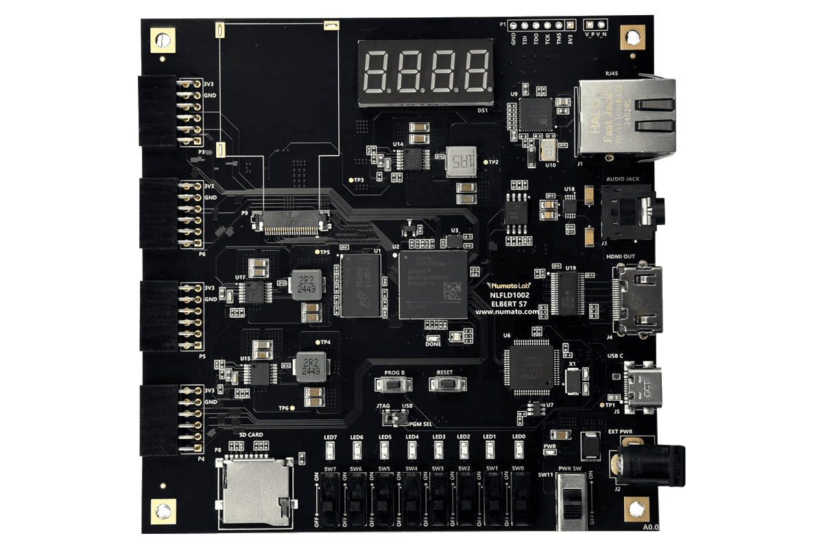
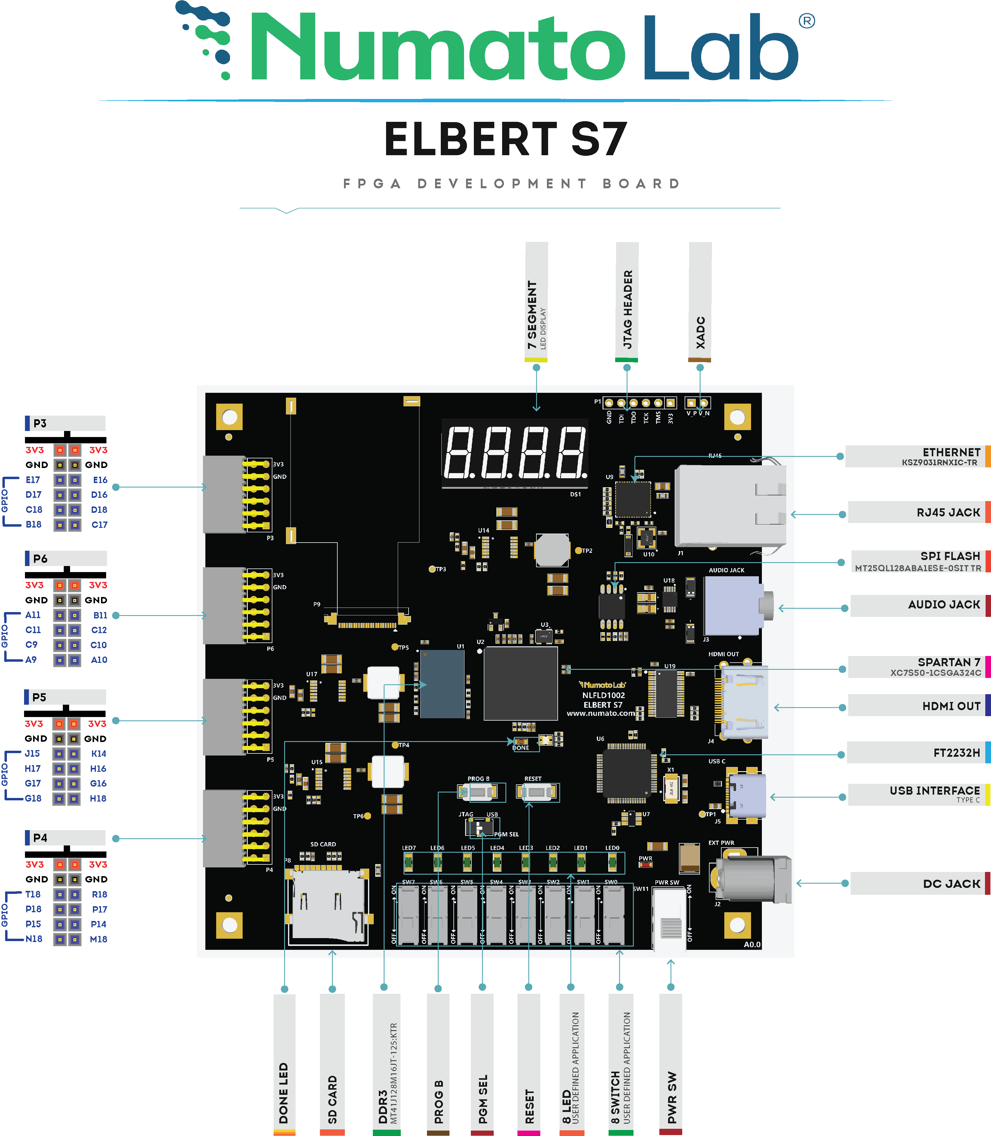
Elbert S7 is a versatile FPGA development board featuring the Spartan-7 FPGA (XC7S50–1CSG324C package), designed for a wide range of applications. This compact and user-friendly board includes QSPI flash for efficient data storage, an FTDI FT2232H for seamless communication, and multiple peripherals for enhanced functionality. It comes equipped with 8 LEDs, 8 Switches for user interaction, Seven-segment display, an SD card slot, HDMI Tx, Gigabit Ethernet, and Audio jack. Additionally, four PMOD headers provide extensive connectivity options, making it ideal for digital signal processing, prototyping, and educational projects. Whether you’re developing advanced applications or learning FPGA design, the Elbert S7 offers a powerful and flexible platform to bring your ideas to life.
Board Features
- FPGA: XC7S50 in CSGA324 package, Speed Grade: -1.
- DDR3: 2Gb DDR3
- Flash memory: 128 Mb Quadbit SPI flash memory.
- 100MHz CMOS Oscillator.
- FTDI FT2232H-based host interface.
- FPGA configuration via JTAG and USB.
- 8 Switches and 8 LEDs for user-defined purposes.
- Four PMODs for user-defined purposes.
- Seven-segment display for numeric output.
- SD Card slot for external storage.
- HDMI Transmitter for video output.
- Gigabit Ethernet for high-speed networking.
- Audio jack for audio applications.
Applications
- Educational tool for Schools and Universities
- Product prototype development
- Accelerated computing integration
- Development and testing of custom embedded processors
- Signal Processing
- Communication devices development
- Video processing
How to use Elbert S7 Development Module
The following sections describe in detail how to use this module.
Hardware Accessories Required
Along with the Elbert S7 Development Board, you may need the items in the list below for easy and fast installation.
- AMD Platform Cable USB II compatible JTAG programmer (optional).
- USB-C type Cable.
- 5V DC power supply (optional).
Wiring Diagram
The following connection diagram should be used for reference only.
USB Interface
The onboard high-speed USB controller helps a Windows/Linux/Mac computer to communicate with this module. Use a USB-C cable to connect it to your PC.
Note: Elbert S7 ships with FT2232H Channel A dedicated to JTAG Programming.
JTAG Connector
JTAG connector allows the FPGA’s JTAG registers to be accessed using a JTAG cable, compatible with the AMD Platform Cable USB.

PROG_B and Reset Buttons
Elbert S7 features a Push-button PROG_B, normally meant to be used as a “PROG_B” signal for configuration reset. Push-button S1 is connected to FPGA pin R8. For enabling manual configuration reset, push-button PROG_B is connected to GND. The user can reconfigure the FPGA manually by pressing the push-button PROG_B.
“PROG_B” controls the configuration logic. When the PROG_B pin is de-asserted, it resets the FPGA and initializes the configuration.
Elbert S7 features a Push-button Reset normally meant to be used as a “Reset” signal for designs running on an FPGA. Push-button Reset is connected to FPGA pin T14. Push-button Reset is active-high. This push button can also be used for any other input and is not just limited to being used as a Reset signal.
DC Power Supply
The board is configured to use power from a DC power supply by connecting it to the External DC Jack. Please refer to the marking on the board for more details. The external power supply should be in the range of +5V, with a sufficient current rating.
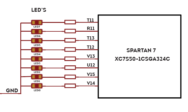
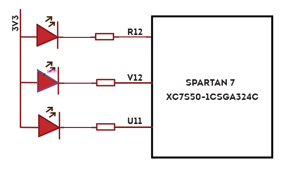
LED's
The board features 8 user-controllable LEDs. These LEDs serve as visual indicators and are commonly used for debugging or representing binary output data. Each LED is connected to a dedicated FPGA pin and can be driven directly using logic outputs.
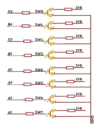
Switches
There are 8 onboard switches that can be used to input binary data or control signals into the FPGA. These inputs are ideal for controlling the flow of a design, setting modes, or triggering actions within a design.
RGB LED
The RGB LED on an FPGA board combines Red, Green, and Blue light-emitting diodes in a single package, allowing the generation of various colours by mixing these primary colours. RGB LEDs are great for status indication or visual feedback in embedded projects.
FT2232H - Spartan-7 (CSGA324) FPGA Connection Details
By default, FTDI channel B is configured for UART.
| Pin Function (245 FIFO) | Pin description | Spartan 7 (CSGA324) Pin No. |
|---|---|---|
| UART RX | IO_L4N_T0_D05_14 | L18 |
| UART TX | IO_L4P_T0_D04_14 | L17 |
PMOD HEADERS
PMOD_0
| Pin No. On The Header | PMOD Pin Name | FPGA PIN | Pin description | Pin No. On The Header | PMOD Pin Name | FPGA PIN | Pin description |
|---|---|---|---|---|---|---|---|
| 6 | VCC | 12 | VCC | ||||
| 5 | GND | 11 | GND | ||||
| 4 | P0_4_P | R18 | IO_L10P_T1_D14_14 | 10 | P0_4_N | T18 | IO_L10N_T1_D15_14 |
| 3 | P0_3_P | P17 | IO_L9P_T1_DQS_14 | 9 | P0_3_N | P18 | IO_L9N_T1_DQS_D13_14 |
| 2 | P0_2_P | P14 | IO_L11P_T1_SRCC_14 | 8 | P0_2_N | P15 | IO_L11N_T1_SRCC_14 |
| 1 | P0_1_P | M18 | IO_L8P_T1_D11_14 | 7 | P0_1_N | N18 | IO_L8N_T1_D12_14 |
PMOD_1
| Pin No. On The Header | PMOD Pin Name | FPGA PIN | Pin description | Pin No. On The Header | Pin No. On The Header | FPGA PIN | Pin description |
|---|---|---|---|---|---|---|---|
| 6 | VCC | 12 | VCC | ||||
| 5 | GND | 11 | GND | ||||
| 4 | P1_4_P | K14 | IO_L23P_T3_15 | 10 | P1_4_N | J15 | IO_L23N_T3_15 |
| 3 | P1_3_P | H16 | IO_L22P_T3_15 | 9 | P1_3_N | H17 | IO_L22N_T3_15 |
| 2 | P1_2_P | G16 | IO_L14P_T2_SRCC_15 | 8 | P1_2_N | G17 | IO_L14N_T2_SRCC_15 |
| 1 | P1_1_P | H18 | IO_L21P_T3_DQS_15 | 7 | P1_1_N | G18 | IO_L21N_T3_DQS_15 |
PMOD_2
| Pin No. On The Header | PMOD Pin Name | FPGA PIN | Pin description | Pin No. On The Header | PMOD Pin Name | FPGA PIN | Pin description |
|---|---|---|---|---|---|---|---|
| 6 | VCC | 12 | VCC | ||||
| 5 | GND | 11 | GND | ||||
| 4 | P2_4_P | B11 | IO_L14P_T2_SRCC_16 | 10 | P2_4_N | A11 | IO_L14N_T2_SRCC_16 |
| 3 | P2_3_P | C12 | IO_L13P_T2_MRCC_16 | 9 | P2_3_N | C11 | IO_L13N_T2_MRCC_16 |
| 2 | P2_2_P | C10 | IO_L11P_T1_SRCC_16 | 8 | P2_2_N | C9 | IO_L11N_T1_SRCC_16 |
| 1 | P2_1_P | A10 | IO_L12P_T1_MRCC_16 | 7 | P2_1_N | A9 | IO_L12N_T1_MRCC_16 |
PMOD_3
| Pin No. On The Header | PMOD Pin Name | FPGA PIN | Pin description | Pin No. On The Header | PMOD Pin Name | FPGA PIN | Pin description |
|---|---|---|---|---|---|---|---|
| 6 | VCC | 12 | VCC | ||||
| 5 | GND | 11 | GND | ||||
| 4 | P3_4_P | E16 | IO_L10P_T1_AD11P_15 | 10 | P3_4_N | E17 | IO_L10N_T1_AD11N_15 |
| 3 | P3_3_P | D16 | IO_L9P_T1_DQS_AD3P_15 | 9 | P3_3_N | D17 | IO_L9N_T1_DQS_AD3N_15 |
| 2 | P3_2_P | D18 | IO_L11P_T1_SRCC_15 | 8 | P3_2_N | C18 | IO_L11N_T1_SRCC_15 |
| 1 | P3_1_P | C17 | IO_L8P_T1_AD10P_15 | 7 | P3_1_N | B18 | IO_L8N_T1_AD10N_15 |
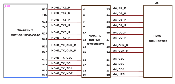
HDMI
The onboard HDMI OUT interface, combined with large DDR3 SDRAM, makes the Elbert S7 board an excellent platform for video rendering. The HDMI OUT interface is buffered using the HDMI buffer TPD12S520D BTR to ensure better signal strength and signal integrity.
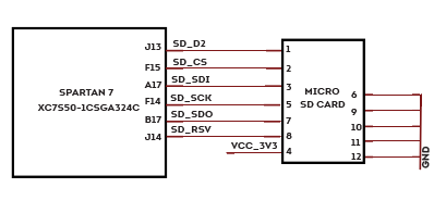
Micro SD
The Elbert S7 board features a micro SD card slot, which allows users to interface with removable flash memory for data storage and retrieval. This is especially useful for embedded applications where storing files, logs, configuration settings, or multimedia content is required.
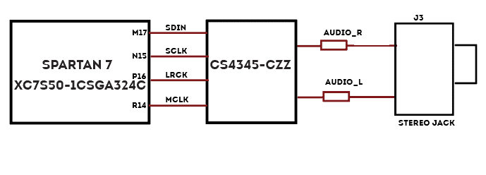
Audio Jack
The Elbert S7 FPGA board is equipped with a 3.5mm stereo Audio jack, enabling audio output to external speakers or headphones. This output is managed by a dedicated digital-to-analog converter (DAC) — the CS4345-CZZ. The inclusion of this audio interface makes the board well-suited for multimedia, audio signal processing, and embedded audio playback applications.
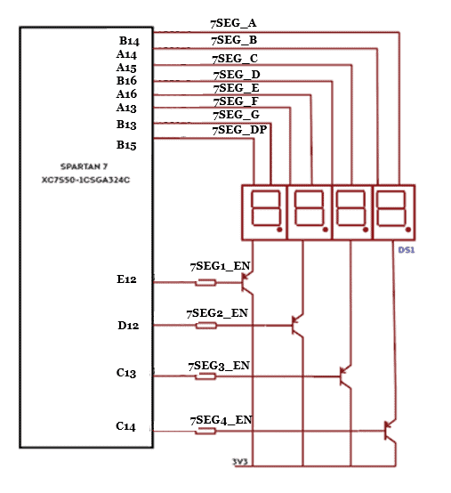
7Segment LED Display
This board includes a four-digit 7-segment LED display, designed with multiplexing to minimize pin usage. Each segment can be individually controlled using 4 Enable pins.
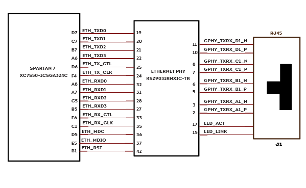
Gigabit Ethernet
Elbert S7 Development Board features KSZ9031RNX, a highly integrated Ethernet transceiver from Microchip that complies with 10BASE-T, 100BASE-TX, and 1000Base-T IEEE 802.3 standards. It supports communication with the Ethernet MAC layer via a standard RGMII interface. It contains a high-performance 10/100/1000T transceiver, and the RGMII interface supports 1000Mbps (1Gbps) operation.
Generating Bitstream Using Vivado
The bitstream can be generated for Elbert S7 in Vivado by following the steps below:
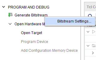
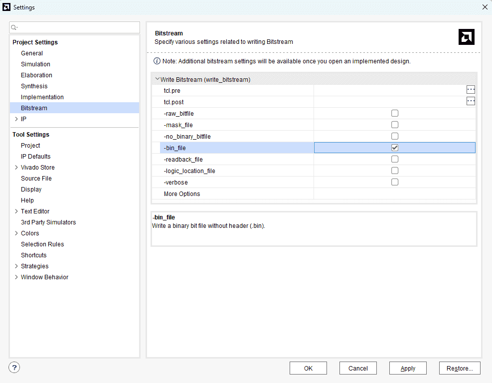
Step 1: It is recommended to generate .bin bitstream file along with .bit bitstream file. Click “Bitstream Settings”.
Step 2: Select “-bin_file*” option in the dialog window and Click OK.
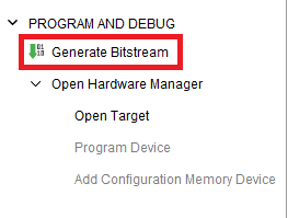
Step 3: Finally click “Generate Bitstream”.
Programming Elbert S7 Using JTAG
Set switch PGM_SEL to JTAG for JTAG programming.
Elbert S7 FPGA features an onboard JTAG connector which facilitates easy reprogramming of SRAM and onboard SPI flash through a JTAG programmer like “AMD Platform cable USB”. The following steps illustrate how to program Elbert S7 using JTAG.
Step 1: By using a JTAG cable, connect the AMD platform cable USB to Elbert S7 and power it up.
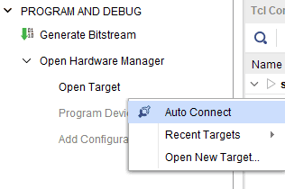
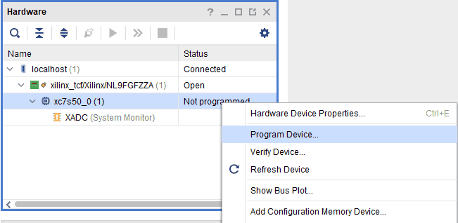
Step 2: Open the Vivado project and open the target by clicking on the “Open Target” in “Open Hardware Manager” in the “Program and Debug” section of the Flow Navigator window. Select “Auto Connect”.
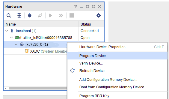
Step 3: If the device is detected successfully, then select “Program Device” after right-clicking on the target device “XC7S50_0” as shown below.
Step 4: In the dialog window that opens up, Vivado automatically chooses the correct bitstream file if the design was synthesized, implemented, and a bitstream was generated successfully. If needed, browse to the bitstream that needs to be programmed to the FPGA. Finally, click “Program”.
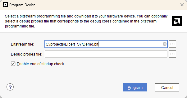
As soon as “Program” is clicked, an orange colored DONE LED (DONE) on Elbert S7 should light up, indicating that the programming process is going on. This LED will turn off when the configuration is complete.
Programming Elbert S7 Using USB-JTAG
Step 1: Ensure that switch PGM_SEL is set to USB and connect the USB Type-C cable to the FPGA board.
Step 2: Click on “Auto connect” under hardware manager, and it will automatically establish the connection.
Step 3: In the dialog window that opens up, Vivado automatically chooses the correct bitstream file if the design was synthesized, implemented, and a bitstream was generated successfully. If needed, browse to the bitstream that needs to be programmed to the FPGA. Finally, click “Program”.
As soon as “Program” is clicked, an orange colored DONE LED (DONE) on Elbert S7 should light up, indicating that the programming process is going on. This LED will turn off when the configuration is complete.
Programming QSPI Flash using Vivado
A .bin or .mcs file is required for programming Elbert S7 onboard QSPI flash.
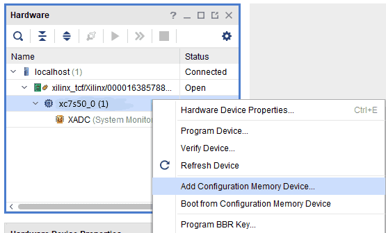
Step 1: Open Vivado project and open the target by clicking on the “Open Target” in “Open Hardware Manager” in the “Program and Debug” section of the Flow Navigator window. Select “Auto Connect”.
Step 2: If the device is detected successfully, then select “Add Configuration Memory Device” after right clicking on the target device “xc7s50_0” as shown below.
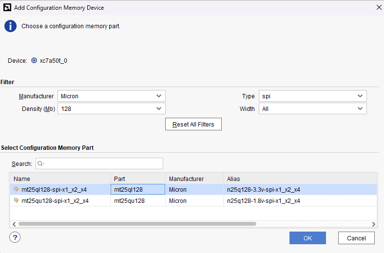
Step 3: Select the memory device “mt25ql128-spi-x1_x2_x4”, then click OK.
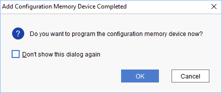
Step 4: After completion of Step 3 the following dialog box will open. Click OK.
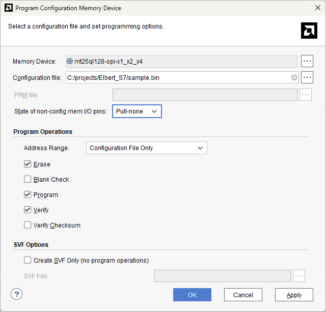
Step 5: Browse to the working .bin file or the .mcs file (whichever applicable) and click OK to program as shown below. If programming is successful, a confirmation message will be displayed.
Technical Specifications
| Parameter * | Value | Unit |
|---|---|---|
| Basic Specifications | ||
| Number of PMODs | 4 | |
| On-board oscillator frequency (ASEM1-100.000MHZ-LC-T) | 100 | MHz |
| Quad SPI Flash Memory (MT25QL128ABA1ESE-0SIT) | 128 | Mb |
| USB Power supply voltage | 5 | V |
| External power Supply voltage (DC jack) | 5 | V |
| Number of LEDs | 8 | |
| Number of switches | 8 | |
| FPGA Specifications | ||
| Internal supply voltage relative to GND | –0.5 to 1.25 | V |
| Auxiliary supply voltage relative to GND | –0.5 to 3.75 | V |
| Output drivers supply voltage relative to GND | –0.5 to 3.75 | V |
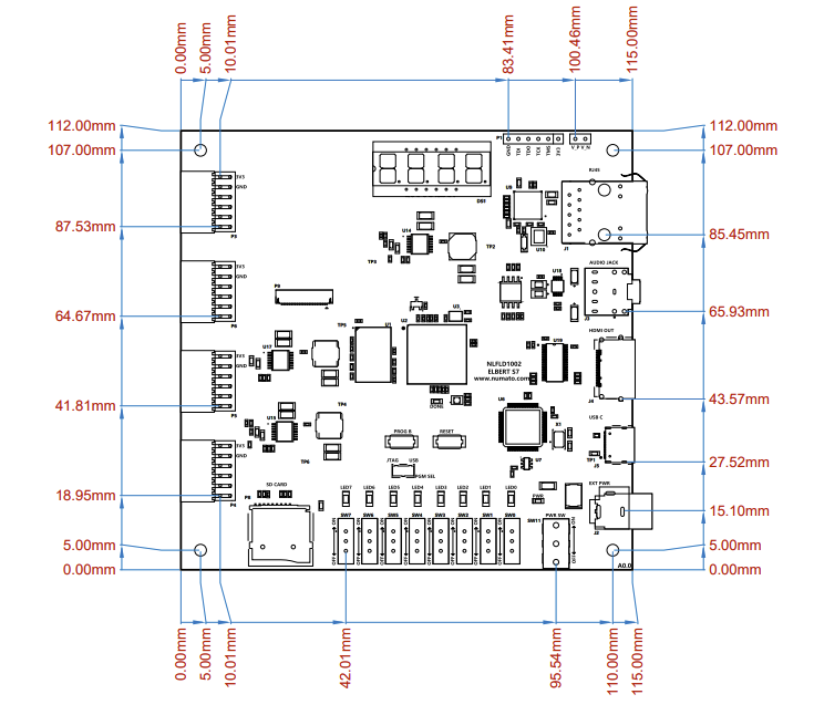
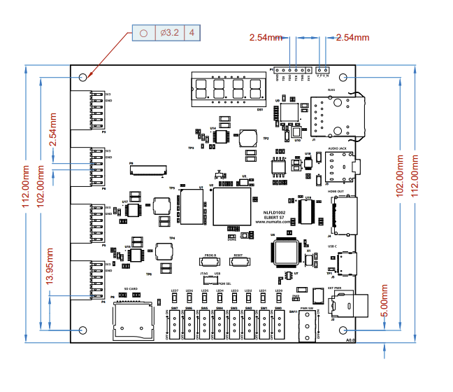
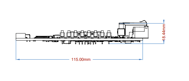
Mechanical Dimensions