Introduction
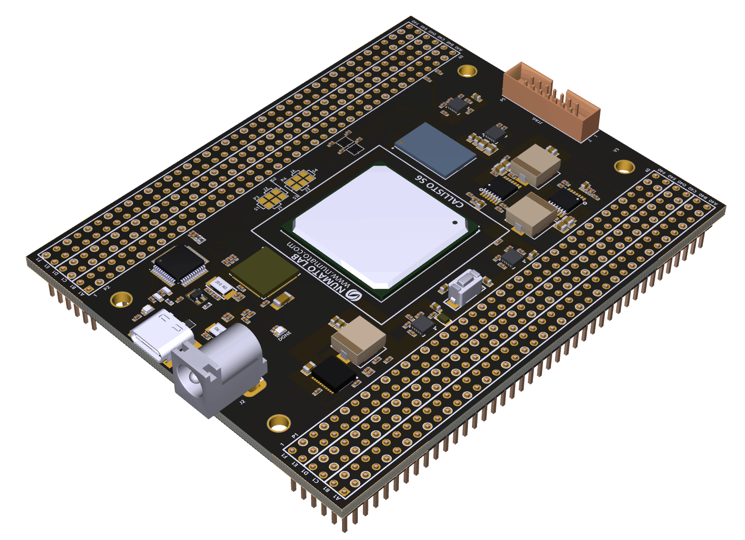
Callisto S6 is an easy to use FPGA Development board featuring the Xilinx Spartan 6 FPGA with 2Gb DDR3 SDRAM. This board contains the Xilinx XC6SLX150– FGG676 FPGA. The high-speed USB 3.1 interface (USB-C connector) provides fast communication interface between FPGA and host PC. The Development board also provides easy access to JTAG signals on a standard Xilinx Platform Cable compatible header. Callisto S6 provides the user the flexibility of adding their own peripherals through IO Expansion Headers.
Board Features
- FPGA: Spartan XC6SLX150 in FGG676 package
- DDR3: 2Gb DDR3 (MT41J128M16HA-125:K or equivalent)
- Flash memory: 128 Mb Quadbit SPI flash memory (N25Q128A13ESE40E)
- 2 x 100MHz CMOS oscillator
- USB 3.1 Gen1 @5Gbps (USB Type-C connector)
- JTAG header for programming and debugging.
- 12V DC power supply
- A Push Button for the reset pin
- 284 IOs for user-defined purposes
- Onboard voltage regulators for single power rail operation
Applications
- Signal Processing
- Product Prototype Development
- Communication devices development
- Educational tool for Schools and Universities
- Development and testing of custom embedded processors
- Accelerated Computing Integration
How to Use Callisto Spartan 6 USB 3.1 Development Board
The following sections describe in detail how to use this module.
Components/Tools Required
Along with the module, you may need the accessories listed below for easy and fast installation:
- 12 V DC Power Supply.
- USB A to USB-C cable (Optional).
- A Xilinx Platform Cable USB II compatible JTAG programmer
Connection Diagram
This diagram should be used as a reference only. For detailed information, see Callisto S6’s schematics and mechanical dimensions at the end of this page. Details of individual connectors are as shown below.
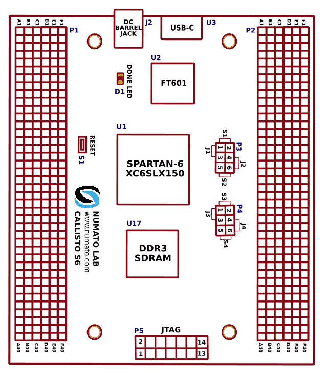
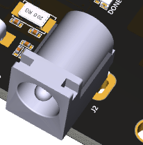
USB Interface
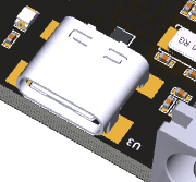 This super speed USB 3.1 interface (USB-C connector) is used to help the host PC to communicate with the module at a very high speed (5Gbps). A USB-A to USB-C cable is used to connect the module to the host PC. It is primarily used to output debug information or as a console for the design running on the board. (the picture on the right shows USB-C connector).
DC Power Supply
 By default, the board is configured to use +5V supply from USB. So an external power is not required unless USB port is unable to supply enough current. USB 3.1 ports are only capable of providing enough current for the module for small designs which require less power. The current requirement for this board largely depends on your application. Please consult FPGA data sheet for more details on power requirements. If for any reason, an external power supply needs to be used for the board, connect the DC power supply. Please refer to the marking on the board for more details. The external power supply should be in the range of +5 to +12V, with sufficient current rating.
Reset Button
Callisto S6 features a Push-button S1 normally meant to be used as “Reset” signal for designs running on FPGA. Push-button S1 is connected to FPGA pin A23. Push-button S1 is active-high. This pushbutton can also be used for any other input and is not just limited to be used as a Reset signal.
JTAG Connector
JTAG connector allows the FPGA’s JTAG registers to be accessed using a JTAG cable, compatible with Xilinx Platform Cable USB. Use this header, to attach JTAG cable for programming and debugging.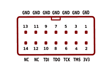
GPIOs
This device is equipped with a maximum of 284 user IO pins that can be used for various custom applications. All user IOs are length matched and can be used as differential pairs.
Header P1
| PIN NO. ON HEADER | Spartan 6 (XC6SLX150-1FGG676) | PIN NO. ON HEADER | Spartan 6 (XC6SLX150-1FGG676) | PIN NO. ON HEADER | Spartan 6 (XC6SLX150-1FGG676) | PIN NO. ON HEADER | Spartan 6 (XC6SLX150-1FGG676) | PIN NO. ON HEADER | Spartan 6 (XC6SLX150-1FGG676) | PIN NO. ON HEADER | Spartan 6 (XC6SLX150-1FGG676) |
|---|---|---|---|---|---|---|---|---|---|---|---|
| A1 | VIN | B1 | VIN | C1 | VIN | D1 | VIN | E1 | VIN | F1 | VIN |
| A2 | GND | B2 | GND | C2 | GND | D2 | GND | E2 | GND | F2 | GND |
| A3 | GND | B3 | B22 | C3 | A22 | D3 | GND | E3 | E20 | F3 | D20 |
| A4 | C21 | B4 | A21 | C4 | GND | D4 | E16 | E4 | F16 | F4 | GND |
| A5 | GND | B5 | B20 | C5 | A20 | D5 | GND | E5 | H15 | F5 | J15 |
| A6 | A19 | B6 | C19 | C6 | GND | D6 | C16 | E6 | D16 | F6 | GND |
| A7 | GND | B7 | A18 | C7 | B18 | D7 | GND | E7 | F15 | F7 | G16 |
| A8 | A17 | B8 | C17 | C8 | GND | D8 | C14 | E8 | D14 | F8 | GND |
| A9 | GND | B9 | A16 | C9 | B16 | D9 | GND | E9 | K15 | F9 | J16 |
| A10 | E14 | B10 | D15 | C10 | GND | D10 | J14 | E10 | G14 | F10 | GND |
| A11 | GND | B11 | A14 | C11 | B14 | D11 | GND | E11 | G13 | F11 | F14 |
| A12 | E12 | B12 | F12 | C12 | GND | D12 | J13 | E12 | K14 | F12 | GND |
| A13 | GND | B13 | C13 | C13 | A13 | D13 | GND | E13 | F13 | F13 | D13 |
| A14 | B12 | B14 | A12 | C14 | GND | D14 | J12 | E14 | H13 | F14 | GND |
| A15 | GND | B15 | A11 | C15 | C11 | D15 | GND | E15 | D12 | F15 | C12 |
| A16 | F11 | B16 | D11 | C16 | GND | D16 | G11 | E16 | H12 | F16 | GND |
| A17 | GND | B17 | B10 | C17 | A10 | D17 | GND | E17 | J11 | F17 | K12 |
| A18 | C9 | B18 | A9 | C18 | GND | D18 | H9 | E18 | H10 | F18 | GND |
| A19 | GND | B19 | B8 | C19 | A8 | D19 | GND | E19 | D10 | F19 | C10 |
| A20 | A7 | B20 | C7 | C20 | GND | D20 | E10 | E20 | F10 | F20 | GND |
| A21 | GND | B21 | D7 | C21 | E8 | D21 | GND | E21 | D8 | F21 | C8 |
| A22 | B6 | B22 | A6 | C22 | GND | D22 | E9 | E22 | F9 | F22 | GND |
| A23 | GND | B23 | A5 | C23 | C5 | D23 | GND | E23 | D5 | F23 | E6 |
| A24 | B4 | B24 | A4 | C24 | GND | D24 | G9 | E24 | F8 | F24 | GND |
| A25 | GND | B25 | G8 | C25 | F7 | D25 | GND | E25 | D6 | F25 | C6 |
| A26 | G7 | B26 | H8 | C26 | GND | D26 | K9 | E26 | J10 | F26 | GND |
| A27 | GND | B27 | G5 | C27 | G6 | D27 | GND | E27 | K8 | F27 | L8 |
| A28 | E5 | B28 | F5 | C28 | GND | D28 | H7 | E28 | J7 | F28 | GND |
| A29 | GND | B29 | E3 | C29 | E4 | D29 | GND | E29 | K6 | F29 | K7 |
| A30 | C3 | B30 | C4 | C30 | GND | D30 | H5 | E30 | H6 | F30 | GND |
| A31 | GND | B31 | B1 | C31 | B2 | D31 | GND | E31 | G3 | F31 | G4 |
| A32 | D1 | B32 | D3 | C32 | GND | D32 | C1 | E32 | C2 | F32 | GND |
| A33 | GND | B33 | F1 | C33 | F3 | D33 | GND | E33 | E1 | F33 | E2 |
| A34 | H1 | B34 | H3 | C34 | GND | D34 | G1 | E34 | G2 | F34 | GND |
| A35 | GND | B35 | J1 | C35 | J2 | D35 | GND | E35 | J3 | F35 | J4 |
| A36 | K1 | B36 | K3 | C36 | GND | D36 | K5 | E36 | J5 | F36 | GND |
| A37 | GND | B37 | L1 | C37 | L2 | D37 | GND | E37 | L9 | F37 | K10 |
| A38 | N1 | B38 | N2 | C38 | GND | D38 | M1 | E38 | M3 | F38 | GND |
| A39 | GND | B39 | GND | C39 | GND | D39 | GND | E39 | GND | F39 | GND |
| A40 | VADJ_B5 | B40 | VADJ_B4 | C40 | VADJ_B0 | D40 | VBATT | E40 | VCC3V3 | F40 | VCC3V3 |
Header P2
| PIN NO. ON HEADER | Spartan 6 (XC6SLX150-1FGG676) | PIN NO. ON HEADER | Spartan 6 (XC6SLX150-1FGG676) | PIN NO. ON HEADER | Spartan 6 (XC6SLX150-1FGG676) | PIN NO. ON HEADER | Spartan 6 (XC6SLX150-1FGG676) | PIN NO. ON HEADER | Spartan 6 (XC6SLX150-1FGG676) | PIN NO. ON HEADER | Spartan 6 (XC6SLX150-1FGG676) |
|---|---|---|---|---|---|---|---|---|---|---|---|
| A1 | J25 | B1 | J26 | C1 | GND | D1 | G20 | E1 | G21 | F1 | GND |
| A2 | GND | B2 | L25 | C2 | L26 | D2 | GND | E2 | K20 | F2 | K21 |
| A3 | H22 | B3 | G22 | C3 | GND | D3 | L20 | E3 | L21 | F3 | GND |
| A4 | GND | B4 | J23 | C4 | J24 | D4 | GND | E4 | H19 | F4 | J20 |
| A5 | K22 | B5 | J22 | C5 | GND | D5 | W17 | E5 | V16 | F5 | GND |
| A6 | GND | B6 | AC20 | C6 | AD21 | D6 | GND | E6 | AF21 | F6 | AE21 |
| A7 | Y18 | B7 | AA19 | C7 | GND | D7 | AB18 | E7 | AA18 | F7 | GND |
| A8 | GND | B8 | AC17 | C8 | AB17 | D8 | GND | E8 | H20 | F8 | H21 |
| A9 | Y16 | B9 | AA17 | C9 | GND | D9 | AC19 | E9 | AD19 | F9 | GND |
| A10 | GND | B10 | W16 | C10 | V15 | D10 | GND | E10 | AE19 | F10 | AF19 |
| A11 | AC14 | B11 | AB15 | C11 | GND | D11 | AD18 | E11 | AF18 | F11 | GND |
| A12 | GND | B12 | AC16 | C12 | AD17 | D12 | GND | E12 | AC15 | F12 | AD15 |
| A13 | Y15 | B13 | AA15 | C13 | GND | D13 | AE15 | E13 | AF15 | F13 | GND |
| A14 | GND | B14 | Y14 | C14 | AA14 | D14 | GND | E14 | AF14 | F14 | AD14 |
| A15 | U15 | B15 | V14 | C15 | GND | D15 | AB13 | E15 | AA13 | F15 | GND |
| A16 | GND | B16 | V13 | C16 | W14 | D16 | GND | E16 | AC13 | F16 | AD13 |
| A17 | U12 | B17 | U13 | C17 | GND | D17 | W13 | E17 | Y13 | F17 | GND |
| A18 | GND | B18 | AB11 | C18 | AA11 | D18 | GND | E18 | AD12 | F18 | AF12 |
| A19 | AA12 | B19 | AC12 | C19 | GND | D19 | AE11 | E19 | AF11 | F19 | GND |
| A20 | GND | B20 | AC11 | C20 | AD11 | D20 | GND | E20 | AD10 | F20 | AF10 |
| A21 | Y10 | B21 | AB10 | C21 | GND | D21 | AE9 | E21 | AF9 | F21 | GND |
| A22 | GND | B22 | AC9 | C22 | AD9 | D22 | GND | E22 | AD8 | F22 | AF8 |
| A23 | AA9 | B23 | AB9 | C23 | GND | D23 | AE7 | E23 | AF7 | F23 | GND |
| A24 | GND | B24 | V12 | C24 | W12 | D24 | GND | E24 | AD6 | F24 | AF6 |
| A25 | V11 | B25 | W11 | C25 | GND | D25 | AE5 | E25 | AF5 | F25 | GND |
| A26 | GND | B26* | Y8 | C26* | Y9 | D26 | GND | E26* | V8 | F26* | W9 |
| A27* | W7 | B27* | W8 | C27 | GND | D27* | AA8 | E27* | AB8 | F27 | GND |
| A28 | GND | B28* | Y6 | C28* | AA7 | D28 | GND | E28* | AB6 | F28* | AB7 |
| A29* | AB5 | B29* | AA5 | C29 | GND | D29* | AC4 | E29* | AD4 | F29 | GND |
| A30 | GND | B30* | AC5 | C30* | AD5 | D30 | GND | E30* | AC3 | F30* | AB4 |
| A31* | AA3 | B31* | AA4 | C31 | GND | D31* | W5 | E31* | Y5 | F31 | GND |
| A32 | GND | B32* | V10 | C32* | W10 | D32 | GND | E32* | U7 | F32* | U8 |
| A33* | T10 | B33* | U9 | C33 | GND | D33* | U5 | E33* | V5 | F33 | GND |
| A34 | GND | B34* | R5 | C34* | T4 | D34 | GND | E34* | U3 | F34* | U4 |
| A35* | T8 | B35* | T6 | C35 | GND | D35* | R10 | E35* | T9 | F35 | GND |
| A36 | AF22 | B36 | AF23 | C36 | AF20 | D36 | AF17 | E36 | AF4 | F36 | AE4 |
| A37 | AE17 | B37 | AD22 | C37 | AD20 | D37 | AD16 | E37 | GND | F37 | AF3 |
| A38 | VCC3V3 | B38 | E21 | C38 | C23 | D38 | A24 | E38 | F20 | F38 | GND |
| A39 | GND | B39 | GND | C39 | GND | D39 | GND | E39 | GND | F39 | GND |
| A40 | VCC3V3 | B40 | VCC3V3 | C40 | VCC3V3 | D40 | VCC3V3 | E40 | VCC3V3 | F40 | VCC3V3 |
* These pins are from Bank 3 whose IOSTANDARD is LVCMOS15 (All other IOs has LVCMOS33 IOSTANDARD)
FT601 - Spartan 6 (FGG676) FPGA Connection Details
| FTDI Pin No. | Pin Function (245 FIFO) | Spartan 6 (FGG676) Pin No. |
|---|---|---|
| 40 | FT_D0 | N22 |
| 41 | FT_D1 | L23 |
| 42 | FT_D2 | M23 |
| 43 | FT_D3 | N23 |
| 44 | FT_D4 | Y24 |
| 45 | FT_D5 | AA24 |
| 46 | FT_D6 | AA25 |
| 47 | FT_D7 | AB24 |
| 50 | FT_D8 | AC25 |
| 51 | FT_D9 | AC24 |
| 52 | FT_D10 | AE26 |
| 53 | FT_D11 | AE25 |
| 54 | FT_D12 | AF25 |
| 55 | FT_D13 | AD24 |
| 56 | FT_D14 | AE24 |
| 57 | FT_D15 | AC23 |
| 60 | FT_D16 | L17 |
| 61 | FT_D17 | K18 |
| 62 | FT_D18 | L18 |
| 63 | FT_D19 | K19 |
| 64 | FT_D20 | L19 |
| 65 | FT_D21 | M21 |
| 66 | FT_D22 | M19 |
| 67 | FT_D23 | N24 |
| 69 | FT_D24 | P24 |
| 70 | FT_D25 | N21 |
| 71 | FT_D26 | N20 |
| 72 | FT_D27 | N19 |
| 73 | FT_D28 | P18 |
| 74 | FT_D29 | P17 |
| 75 | FT_D30 | R18 |
| 76 | FT_D31 | R17 |
| 4 | FT_BE0 | P26 |
| 5 | FT_BE1 | R26 |
| 6 | FT_BE2 | T26 |
| 7 | FT_BE3 | U26 |
| 8 | FT_TXE | V26 |
| 9 | FT_RXE | W26 |
| 11 | FT_WR | Y26 |
| 12 | FT_RD | AA26 |
| 13 | FT_OE | AB26 |
| 15 | FT_RST | AC26 |
| 16 | FT_WK | AD26 |
| 58 | FT_CLK | U25 |
Driver Installation
This product requires a driver to be installed for proper functioning when used with Windows. The D3XX driver can be downloaded from http://www.ftdichip.com/Drivers/D3XX.htm. Windows Users should download and run the latest WHQL Certified executable file that will prompt to install the FTDI CDM drivers.
Generating Bit Stream for Callisto S6
HDL design needs to be converted to bitstream before it can be programmed to FPGA. Once the HDL is synthesized, it is easy to create a bit stream out of it. Please follow the steps below to generate bit stream from your design using ISE Web Pack.
Step 1: Right click on the “Generate Programming File” option in “Processes” window.
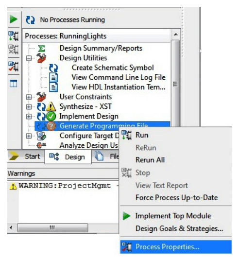
Step 2: Select “Process Properties” from the pop-up menu. In the dialog box, select “Create Binary Configuration File” and click “Apply”.
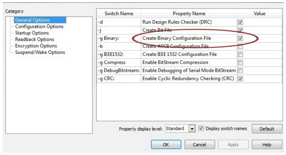
Step 3: Click “OK” to close the dialog box. Right click on “Generate Programming File” option again and select “Run”. Now you will be able to find a “.bit” and a .bin files in the project directory and that file can be used for Callisto S6 configuration.
Powering Up Callisto S6
Callisto S6 is factory configured to be powered directly from USB port so make sure that you are using a USB port that can power the board properly. It is recommended to connect the board directly to the PC instead of using a hub. It is practically very difficult to estimate the power consumption of the board, as it depends heavily on your design and the clock used. XILINX provides tools to estimate the power consumption. In any case, if power from USB is not enough for your application, external supply can be applied to the board. Callisto S6 requires three different voltages, a 3.3V, a 1.8V supplies and a 1.2V supply. Onboard regulators derive these voltages from the USB/Ext power supply.
Programming Callisto S6 using JTAG
Callisto Spartan6 module features onboard JTAG connector which facilitates easy reprogramming of SRAM and on-board SPI flash through JTAG programmer like “XILINX Platform-cable usb”. Programming Callisto S6 using JTAG requires “XILINX ISE iMPACT” software which is bundled with XILINX ISE Design Suite. To program the SPI flash we need a “.mcs” file needs to be generated from the “.bit” file. Steps for generating “.mcs” file are as below. Programming FPGA SRAM does not require a “.mcs” file to be generated.
Generating “.mcs” file for Callisto S6
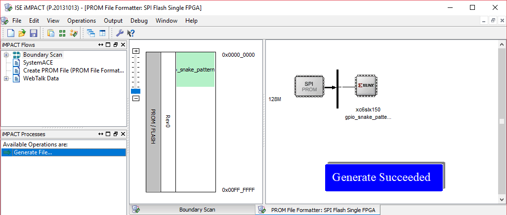
Step 1: Open ISE iMPACT. Click on “Create PROM file(PROM file formatter)”. In the dialog box, select “Configure Single FPGA” in storage device type. Then click on the green arrow on the right side.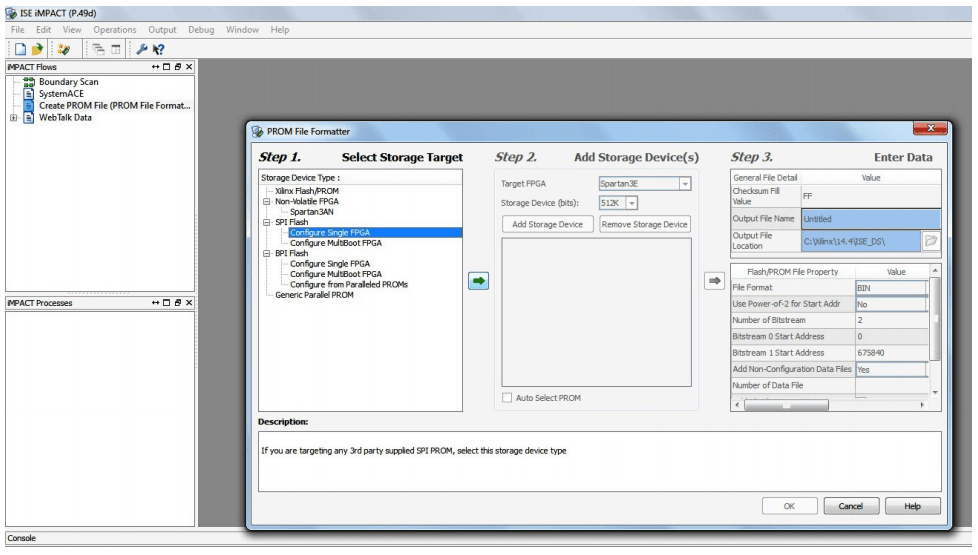
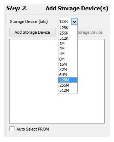
Step 2: Select 128M in Storage Device (bits).Now click on “Add Storage Device”, then the green arrow on the right side.
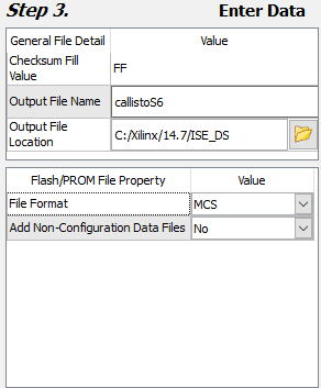
Step 3: Set an output file name and the output file location (the “.mcs” file will be generated at this location which will be required later for programming the FPGA), then click OK twice, then select the “.bit” file we already generated then click Open and click NO when it prompts to add another device file.
Step 4: Double-click on “Generate File”. “Generate Succeeded” will be displayed as shown in fig below if the “.mcs” the file is generated successfully.
Programming Onboard SPI flash Using ISE iMPACT
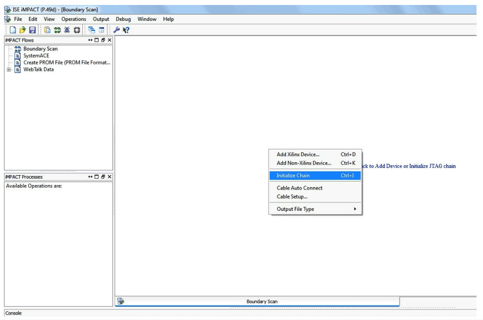
Step 1: Open ISE iMPACT. Click on “Boundary Scan” in the iMPACT flows window on the left top corner. Then right-click on the window panel on the right. Select “Initialize Chain”.
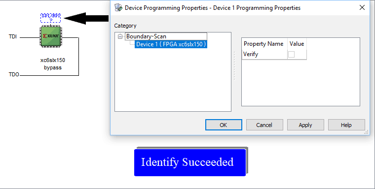
Step 2: If the device is detected properly you will get a pop-up window as shown below, Click OK. Then right-click on the SPI/BPI (next to the black arrow in the below fig.), select Add SPI/BPI Flash.
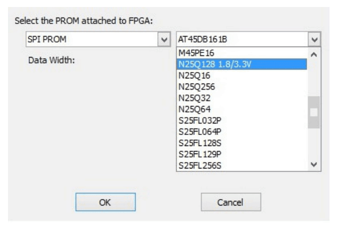
Step 3: Select the “.mcs” file we already created and click OK. Now choose “N25Q128” in the dialogue box appeared, then click OK.
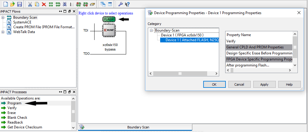
Step 4: Click on “Flash”, Double Click on Program, select OK. If the programming is successful, a confirmation message will be displayed.
Technical Specifications
| Parameter * | Value | Unit |
|---|---|---|
| Basic Specifications | ||
| Number of GPIOs | 284 | |
| On-board oscillator frequency (ASEM1-100.000MHZ-LC-T) | 100 (x2) | MHz |
| DDR3 SDRAM (MT41J128M16HA - 125 or Equivalent) | 2 | Gb |
| Quad SPI Flash Memory (N25Q128A13ESE40E) | 128 | Mb |
| Power supply voltage (USB or External) | 5 - 12 | V |
| FPGA Specifications | ||
| Internal supply voltage relative to GND | –0.5 to 1.32 | V |
| Auxiliary supply voltage relative to GND | –0.5 to 3.75 | V |
| Output drivers supply voltage relative to GND | –0.5 to 3.75 | V |
* All parameters considered nominal. Numato Systems Pvt Ltd reserves the right to modify products without notice.
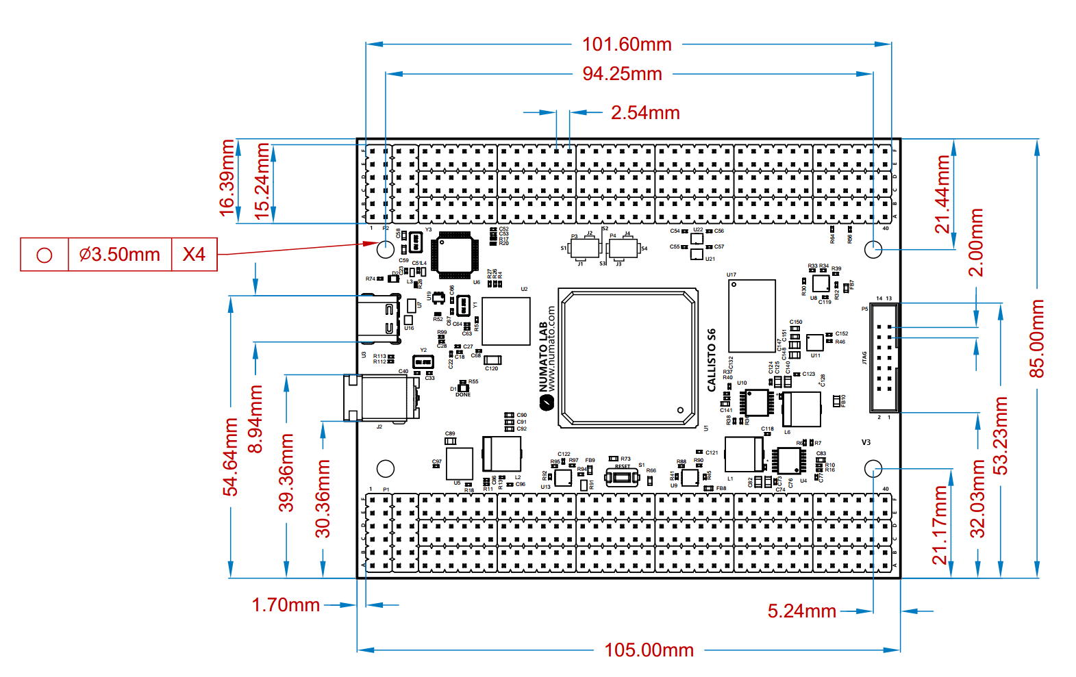
Physical Dimensions