Introduction
Designing and building an FPGA development board that has two BGA devices was challenging enough. But what came next did seem equally challenging to us in the beginning. That challenge was testing the functionality of the DDR interface. We had no prior experience of successfully building a board with a DDR device. And those who know about the DDR interface can tell that it is not very easy implementing. Thanks to the memory controller built into Spartan 6 FPGAs and Xilinx MIG tool which helped us generate sample code. Searching through websites we found out that there are not many tutorials and good example projects that are easy to follow. And we thought we should share with our readers what we learned. This blog post is an attempt to help beginners get their first DDR interfacing project up and running quickly, and without writing any code at all. This is possible because Xilinx provides a complete and working example project along with their IP. So we won’t write any code or learn how DDR works in this tutorial. This is not intended to be a tutorial on the working of DDR or FPGAs, rather a quick practical tutorial on how to run your first project that uses DDR memory.
Xilinx Spartan 6 FPGAs has hard DDR memory controller built-in which makes working with DDR easier. And the ISE Core Generator supports configuring and generating code for the memory controller. The software wizard that helps with configuring and generating code for the memory controller is called MIG (Memory Interface Generator). We will use MIG to generate code and will build an example project that is generated. And program and test the code on a Saturn Spartan 6 FPGA module.
A short introduction to the Saturn Spartan 6 FPGA module before we proceed to the rest of the steps. Saturn is a low-cost FPGA development platform created by Numato Lab. Saturn has a Xilinx Spartan 6 FPGA in CSG324 package and a 512Mbit LPDDR memory with lots of GPIOs for external interfacing. It has an SPI flash memory for configuration storage and 100MHz crystal oscillator as a clock source. User manual and other tools for Saturn are available at the product page. Saturn is an open source design and all design source files and other resources are available for download at Numato Lab’s GitHub Repository.
Memory Controller IP configuration and code generation using MIG
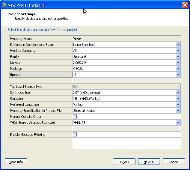
Ok, that is enough introduction, let’s get back to work. The only piece of software you will need is Xilinx ISE which is available for download for free from http://www.xilinx.com. Start ISE and select a new project from the File menu. The project wizard will pop up. Type in a project name and path on the first page. Select the appropriate FPGA device on the second page. Saturn has a Spartan 6 LX9 device (XC6SLX9). Settings, as shown in the image below, should work fine.
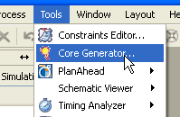
Click next and finish the wizard. Surprisingly we are not going to create or add any source files to the project and our use of ISE ends once we start the Coregen tool. To start Coregen tool, go to the Tools menu and select “Core Generator”.
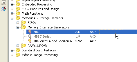
If Core Generator does not create a project automatically, create a project by selecting File>New Project. You will need to select the FPGA and its package when creating the project. Select Verilog as a design entry method. This is to make sure that the Core Generator generates code in Verilog. In the IP catalog window, Find MIG under “Memory & Storage Elements” Category.
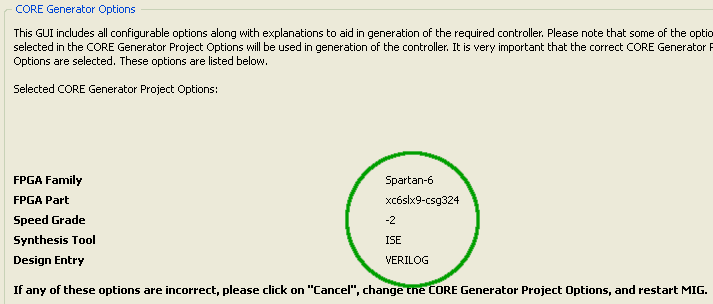
Double click to run Memory Interface Generator wizard. On the first screen, make sure that the selected FPGA device and other settings are correct. The settings should look like in the image below (if you are using the LX9 version of Saturn).
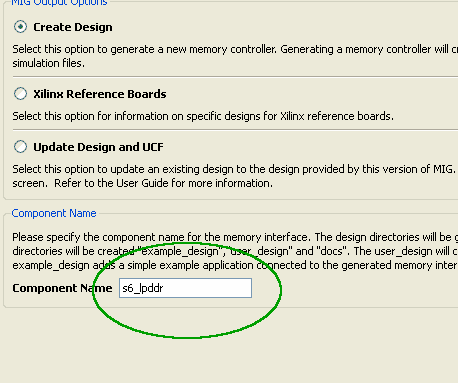
Click next to proceed to the next screen and type in a component name if necessary. Leaving the default name should work fine as well. For the sake of clarity, I’ll call my component “s6_lpddr”. Please replace this with the component name you chose when “s6_lpddr” appears later in this tutorial.
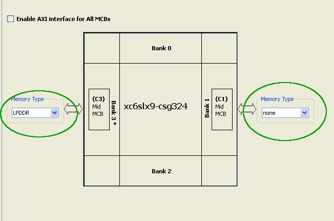
Click next to go to screen three of the wizard. Leave all options unchanged and proceed to screen 4. This screen is where we select the type of DDR memory and tell the wizard where it is connected. Spartan 6 LX9 device has two memory controllers available. On Saturn FPGA module, the LPDDR device is connected to Bank 3 of the FPGA. Select LPDDR from the combo box corresponding to Bank 3. Leave Bank 1 settings unchanged. Settings on this page should look like as in the image below.
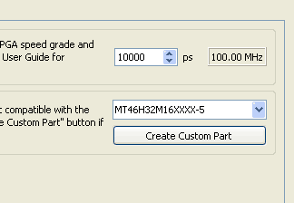
Click next to go to the next screen. This is the place where we select the DDR memory device and its operating frequency. Saturn has onboard LPDDR memory which is Micron MT46H32M16 or equivalent. This device supports DDR clock up to 166MHz. Select MT46H32M16 memory device and set the clock period to 10,000. Clock period 10,000 corresponds to 100MHz DDR clock frequency. Though the DDR device supports up to a 166MHz clock, we will use 100MHz to avoid the complication of messing with the PLL settings later. Saturn has a 100MHz clock source and by using the same frequency for DDR clock, we can leave the PLL settings generated by MIG as is. Below is the image with the correct memory part and frequency selected.
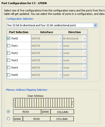
Click next to proceed to the next screen and leave all settings to its defaults. Click next again to proceed to the port configuration screen. Select Port 0 and leave rest of the ports unchecked as shown below.
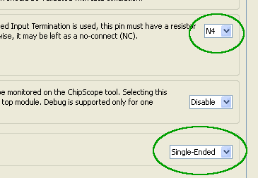
Click next to proceed to the arbitration configuration page. Since we are using only one port, there are no parameters to change on this screen. Click next again to proceed to FPGA Options screen. Select N4 as RZQ pin location and select Single Ended as a system clock input. See image below with correct settings.
Click the next button a few more times and finish. Core Generator will generate a bunch of files. These files can be found under the directory \ipcore_dir\s6_lpddr (Assuming you used the name “s6_lpddr” for the auto-generated component). You will see three folders here, docs, example_design and user_design. docs folder has some very important documentation that can be used to learn more about Spartan 6 Memory Controller and the IP generated by MIG. Keep them for a later read.
Editing user constraints
Right now we are going to use the example design generated by MIG. The example design can be found (unsurprisingly) under the folder example_design. There are a few folders and files inside the example_design folder. RTL folder has all the Verilog files generated by MIG. par folder contains some batch files and scripts to build the example design. The user constraints seem to be autogenerated to match with Xilinx’s own development boards. Some changes are necessary to make the autogenerated code work with Saturn. Before building the project, we need to do the following.
- Edit the ucf file to make it usable with Saturn
- Configure the build environment to generate a binary configuration file
Go to par folder and find example_top.ucf. Open example_top.ucf using any text editor of your choice. Make the following changes.
- Change the line CONFIG VCCAUX=2.5; to CONFIG VCCAUX=3.3; This change is necessary because Saturn uses 3.3V for VCCAUX.
- Change the following lines
NET  "error"                                    IOSTANDARD = LVCMOS18;
NET  "calib_done"                               IOSTANDARD = LVCMOS18;
NET  "calib_done"                               LOC = "B2";
NET  "error"                                    LOC = "A2";
To
NET  "error"                                    IOSTANDARD = LVCMOS33;
NET  "calib_done"                               IOSTANDARD = LVCMOS33;
NET  "calib_done"                               LOC = "K13";
NET  "error"                                    LOC = "K12";
Above changes will make the “error” and “calib_done” pins operate at LVCMOS33 IO standard and assign the nets to K12 and K13 of FPGA which can be accessed easily on the expansion connector.
- Change the lines
NET  "c3_sys_clk"                                  IOSTANDARD = LVCMOS25;
NET  "c3_sys_rst_n"                                IOSTANDARD = LVCMOS18;
To
NET  "c3_sys_clk"                                  IOSTANDARD = LVCMOS33;
NET  "c3_sys_rst_n"                                IOSTANDARD = LVCMOS33;
Above change will set the IO standards for clock input and reset input to LVCMOS33. This is again because the bank that this IO belongs is powered by 3.3V rail.
4. Add a line NET “c3_sys_rst_n” PULLDOWN; right after the above change.
Enabling pull down on the reset pin. This will keep the DDR IP out of reset without having to use any external components. Despite the name “c3_sys_rst_n”, MIG seems to be configuring reset input as active high.
5. Change “c3_sys_clk” and “c3_sys_rst_n” pin assignments as below.
NET  "c3_sys_clk"                                LOC = "V10";
NET  "c3_sys_rst_n"                              LOC = "M13";
This code change will assign correct IO pads for clock input and reset input.
We are done with the changes in the ucf file now. This may seem difficult but easy enough if done carefully. It is a good idea to back up your original ucf file before saving the changes just in case if you want to go back and restart again.
Building the code
Next step is to modify the build environment to generate a binary configuration file. This is a very easy step to do. Find the file mem_interface_top.ut and open it in a text editor. Find the line “-g Binary:no” and change it to “-g Binary:yes” and save.
Now we are ready to build the project. Before building the project, make sure that the path to Xilinx build tools is added to the PATH environment variable. Usually, the path is C:\Xilinx\<ISE Version>\ISE_DS\ISE\bin\nt assuming ISE is installed on C: drive.
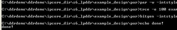
Now run the batch file ise_flow.bat by double-clicking the file or by using the command prompt. If everything went fine so far, the batch file will run the necessary tools to build the project and you will end up with a “Done” message and a bunch of new files in the par folder. The message should look like in the image below.
If the build process fails, refer to ise_flow_results.txt for more details on the causes of failure. You should see the file “example_top.bin” in par folder if build succeeded. This is the file we are going to program Saturn Spartan 6 Module with.
Configuring Saturn and testing
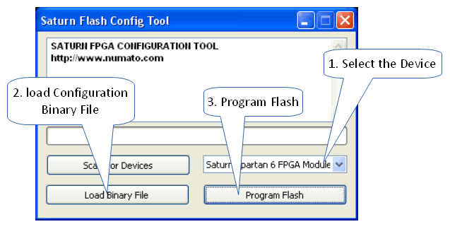
Programming Saturn Spartan 6 FPGA development board is very easy. Download the latest version of the Configuration Downloader Application from the product page. Run the executable, no installation required. Load the binary file and program the flash as illustrated in the image below.
Watch the log window and confirm the configuration binary file is downloaded successfully. Now we are ready to test if the memory interface is working.
Testing if the example program we built, is very easy to do. You may remember we changed a few lines in the ucf file. Below are two of those lines.
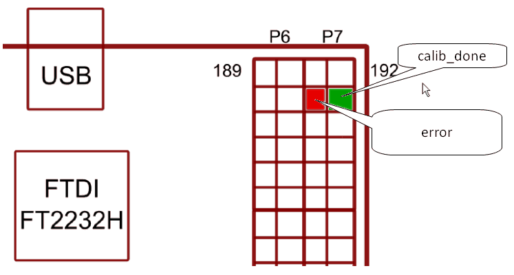
NET  "calib_done"                            LOC = "K13";
NET  "error"                                 LOC = "K12";
The first line assigns the FPGA pin K13 to the net “calib_done” net and the second line assigns FPGA pin K12 to “error” net. To verify proper functioning of the example program, all that we need to do is to check and make sure that “calib_done” goes high after power-up, indicating successful completion of initial calibration and “error” stays low. This check can be done by using a simple multi-meter of an oscilloscope. Referring to the Saturn Spartan 6 FPGA module user guide, it is easy to find out that K12 (GPIO-P13) and K13 (GPIO-N13) are available at pin no. 187 and pin no. 188 of the expansion connector respectively. The picture below illustrates the pins to check on the Saturn Spartan 6 FPGA module expansion connector.
If you have observed calib_done going high and error stays low for a while, congratulations to you, you’ve got your Spartan 6 DDR SDRAM test project working. Thanks to Xilinx Memory Interface Generator for generating complete ready to go code.
I’m hoping I kept the promise of completing this project without writing any code with the minor exception of editing the user constraints file.
Looking forward to reading your comments and suggestions below.
Just purchased a Saturn and intend to use ddr so many thanks for this information.
March 8, 2019 at 10:16 pm