Introduction
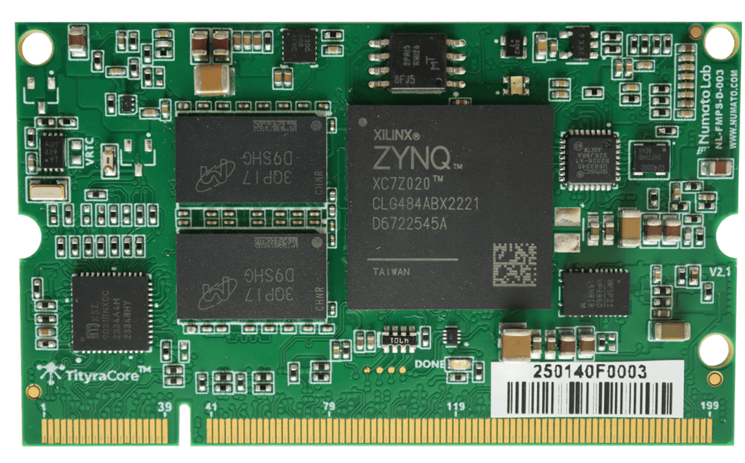
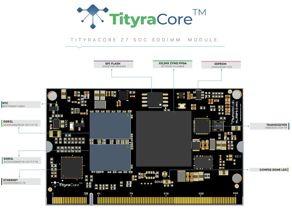
TityraCore Z7 SoC SODIMM incorporates the AMD Zynq XC7Z020 chip, seamlessly integrating programmable logic with a dual-core ARM Cortex-A9 processor. This integration provides a potent blend of hardware and software processing capabilities, all within a single chip. Zynq series features a hard System on Chip (SoC) with an ARM core. The range of peripherals offered includes an extensive array of functionalities, such as UARTs, Ethernet controllers, USB ports, timers, interrupt controllers, and various other features. It has a seamless integration of the Processing System(PS) with the Programmable Logic (PL) in which the interaction between them is enabled by a high-bandwidth interface, ensuring communication and efficient data transfer between them. TityraCore Z7 SoC SODIMM is specifically designed for the development and integration of FPGA-based accelerated features into other larger designs. It opens up a vast realm of possibilities for implementing innovative solutions across various applications.
Board features
- Device: XC7Z020 in CLG484 package, Speed Grade: -1
- SDRAM: 1 GB DDR3L.
- Flash memory: 128 Mb Quad bit SPI flash memory.
- 33 MHz CMOS oscillator
- 50 MHz CMOS oscillator
- Gigabit Ethernet.
- Real Time Clock.
- CAN BUS.
- MIPI interfacing.
- High-Speed USB 2.0 OTG interface.
- JTAG and USB programming.
- Micro SD card for memory expansion
- 8 GB eMMC
Application
- Product Prototype Development
- Accelerated computing integration
- Custom Embedded platform
- Signal Processing
- Communication devices development
- Educational tool for Schools and Universities
Components/Tools required
Along with the module, you may need the items in the list below for easy and fast installation.
- TityraCore SoC Carrier.
- Micro-B cable.
- USB-C cable
- AMD Platform Cable USB or compatible JTAG programmer. (optional)
- DC Power supply (12V).
Wiring Diagram
Reference clock
Bank Pin No. Signal Name Function
500 F7 PS_CLK_500 33.33 MHz CLK
34 W17
IO_L13P_T2_MRCC_33
50 MHz CLK
Reset
Bank Pin No. Signal name Function
501 C9 PS_SRST_B_501 n RST IN
500 B5 PS_POR_B_500 Program B
34 M14 IO_L6N_T0_VREF_34 IO_RST
DDR3L SDRAM
TityraCore Z7 SoC SODIMM includes DDR3L memory technology which is the third generation of DDR memory technology designed to operate at lower voltage levels (1.35 V) compared to standard DDR3 modules.
UART
TityraCore Z7 SoC SODIMM supports UART pins connected to Bank 501 of PS and works at 1.8V voltage.
Bank Pin No: Signal Name Function
502 D11 PS_MIO48_501 UART_TX
502 C14 PS_MIO49_501 UART_RX
QSPI Flash
The TityraCore Z7 SoC SODIMM has 128 Mb of Quad bit SPI flash memory. It is a serial NOR flash which operates at the voltage of 3.3 V. It is connected to QSPI controller of the PS and serves as the default primary boot device. Memory size of QSPI flash memory can be expanded to 8GB using eMMC flash.
Bank Pin No. Signal Name Function
500 A1
PS_MIO1_500 SPI_CS_N
500 A2
PS_MIO2_500 SPI_DQ[0]
500 F6 PS_MIO3_500 SPI_DQ[1]
500 E4 PS_MIO4_500 SPI_DQ[2]
500 A3 PS_MIO5_500 SPI_DQ[3]
500 A4 PS_MIO6_500 SPI_SCK
MicroSD Card
The TityrCore Z7 SoC SODIMM have microSD card feature that can be incorporated in the carrier board. SD Card can be used to store non-volatile external memory and also can be used as a mean for secondary booting. It is directly connected to the SD0 controller of the PS MIO bank and operates at 1.8 V. The SD card can be accessed through the SD card connector in the carrier board.
Bank Pin No. Signal Name Function
501 E14 PS_MIO40_501 SD0_CLK
501 C8 PS_MIO41_501 SD0_CMD
501 D8 PS_MIO42_501 SD0_DAT0
501 B11 PS_MIO43_501 SD0_DAT1
501 E13 PS_MIO44_501 SD0_DAT2
501 B9 PS_MIO45_501 SD0_DAT3
eMMC Flash
TityraCore Z7 SoC SODIMM supports 8 GB of eMMC flash memory for additional storage which is expandable up to 64 GB. It operates at a voltage level of 3.3 V and is connected to SD1 controller of the PS MIO bank . It has four data lines and function as a secondary boot device.
Bank Pin No. Signal Name Function
500 G7 PS_MIO10_500 eMMC_DAT0
500 B4 PS_MIO11_500 eMMC_CMD
500 C5 PS_MIO12_500 eMMC_CLK
500 A6 PS_MIO13_500 eMMC_DAT1
500 B6 PS_MIO14_500 eMMC_DAT2
500 E6 PS_MIO15_500 eMMC_DAT3
Ethernet
TityraCore Z7 SoC SODIMM implements single-Chip 10/100/1000 Mbps Ethernet Transceiver, with 1.8 V IO operating voltage using Gigabit ethernet PHY “KSZ9031RNX”. It provides the Reduced Gigabit Media Independent Interface (RGMII) and is connected to the ENET0 interface of PS MIO bank in Zynq-7000 SOC. It operates in 1.8 V and also supports Link and Activity LED indication in carrier board. Ethernet functionality can be accessed through RJ45 Jack in the carrier board.
Bank Pin No. Signal Name Function
501 D6 PS_MIO16_501 ETH_TXCLK
501 E9 PS_MIO17_501 ETH_TXD0
501 A7 PS_MIO18_501 ETH_TXD1
501 E10 PS_MIO19_501 ETH_TXD2
501 A8 PS_MIO20_501 ETH_TXD3
501 F11 PS_MIO21_501 ETH_TXCTL
501 A14 PS_MIO22_501 ETH_RXCLK
501 E11 PS_MIO23_501 ETH_RXD0
501 B7 PS_MIO24_501 ETH_RXD1
501 F12 PS_MIO25_501 ETH_RXD2
501 A13 PS_MIO26_501 ETH_RXD3
501 D7 PS_MIO27_501 ETH_RXCTL
501 D10 PS_MIO52_501 ETH_MDC
501 C12 PS_MIO53_501 ETH_MDIO
USB 2.0 OTG
TityraCore Z7 SoC SODIMM support high speed USB 2.0 On-The-Go (OTG) transceiver with 24 MHz operating frequency. It uses “USB3340” ULPI transceiver and supports both device and host modes(Default HOST Mode). The ULPI (UTMI+ Low Pin Interface) protocol is utilized to establish a connection between MIO pins and the PHY component. It is connected to the OTG controller of PS MIO bank and works at 1.8V voltage.
The VBUS and USB ID pins play crucial roles in determining whether the OTG operates in Host mode, Device mode, or OTG mode.
Note: While shipping the board, the default configuration is set to Host mode. This setting can be changed as per the user’s requirements.
Bank Pin No. Signal Name Function
501 A12 PS_MIO28_501 USB_D4
501 E8 PS_MIO29_501 USB_DIR
501 A11 PS_MIO30_501 USB_STP
501 F9 PS_MIO31_501 USB_NXT
501 C7 PS_MIO32_501 USB_D0
501 G13 PS_MIO33_501 USB_D1
501 B12 PS_MIO34_501 USB_D2
501 F14 PS_MIO35_501 USB_D3
501 A9 PS_MIO36_501 USB_CLK
501 B14 PS_MIO37_501 USB_D5
501 F13 PS_MIO38_501 USB_D6
501 C13 PS_MIO39_501 USB_D7
MAC EEPROM
TityraCore Z7 SoC SODIMM features MAC ID EEPROM, which is a memory chip that stores the unique MAC address of a network interface. It is a non-volatile memory that interfaces with PS MIO Bank501 of Zynq-7000 AP SoC. It operates at a voltage of 1.8 V.
Bank Pin No Signal name Function
501 D12 PS_MIO46_501 MAC_SCL
501 B10 PS_MIO47_501 MAC_SDA
CAN
The TityraCore Z7 SoC SODIMM facilitates CAN communication via the PS CAN controller and provides a versatile and effective means of establishing connections with diverse peripheral devices utilizing the CAN protocol. It has a operating voltage of 1.8 V.
Bank Pin No. Signal Name Function
501 D13 PS_MIO50_501 CAN_RX
501 C10 PS_MIO51_501 CAN_TX
Real Time Clock
TityraCore Z7 SoC SODIMM includes Real Time Clock (RTC), an integral part of electronic devices that operates independently of the device to accurately track real-world time. It is connected to PL Bank33 and has an operating voltage of 3.3 V. The carrier should include a coin cell battery to provide low power in the absence of an external power supply.
Bank Pin No Signal Name Function
33 W18 IO_L13N_T2_MRCC_33 RTSCL
33 W16 IO_L14P_T2_MRCC_33 RTSDA
RGB LED
The TityraCore SoC SODIMM includes an RGB LED for user requirements. It is connected to PL Bank33 and has an operating voltage of 3.3 V.
Bank Pin No. Signal Name Function
33 Y16 IO_L14N_T2_SRCC_33 LED0
33 U15 IO_L15P_T2_DQS_33 LED1
33 U16 IO_L15N_T2_DQS_33 LED2
SODIMM Connector Pinout
Signal Name FPGA Pins SODIMM Pin(Top) SODIMM Pin(Bottom) FPGA Pins Signal Name
GND 1 2 GPHY_ATXRX_P
n_RST_IN C9 3 4 GPHY_ATXRX_N
GND 5 6 GPHY_BTXRX_P
MIPI_LANE0_P M21 7 8 GPHY_BTXRX_N
MIPI_LANE0_N M22 9 10 GND
MIPI_LANE1_P N22 11 12 GPHY_CTXRX_P
MIPI_LANE1_N P22 13 14 GPHY_CTXRX_N
MIPI_CLK_P M19 15 16 GPHY_DTXRX_P
MIPI_CLK_N M20 17 18 GPHY_DTXRX_N
CAM_PWUP N20 19 20 GND
CAM_CLK N19 21 22 GPHY_ACTIVITY_LED1
CAM_SCL P18 23 24 VCC3V3
CAM_SDA P17 25 26 GPHY_LINK_LED2
GND 27 28 E4 SPI_DQ2
FPGA_TDI H13 29 30 A3 SPI_DQ3
FPGA_TDO G14 31 32 VCC3V3
FPGA_TMS G12 33 34 M15 FMC_PG_ALL
FPGA_TCK G11 35 36 VCC3V3
UART_TX D11 37 38 T11 PROGRAM_B
UART_RX C14 39 40 GND
GND 41 42 C10 CAN_TX
SD0_CLK E14 43 44 D13 CAN_RX
SD0_CMD C8 45 46 VCC3V3
GND 47 48 A18 PL_IO_L10_T1_AD11_35_P
SD0_DATA0 D8 49 50 A19 PL_IO_L10_T1_AD11_35_N
SD0_DATA1 B11 51 52 B16 PL_IO_L8_T1_AD10_35_P
SD0_DATA2 E13 53 54 B17 PL_IO_L8_T1_AD10_35_N
SD0_DATA3 B9 55 56 A16 PL_IO_L9_T1_DQS_AD3_35_P
PRESENT M16 57 58 A17 PL_IO_L9_T1_DQS_AD3_35_N
IO_L8_T1_34 J22 59 60 VCC3V3
PL_IO_L11_T1_SRCC_35_P C17 61 62 C15 PL_IO_L7_T1_AD2_35_P
PL_IO_L11_T1_SRCC_35_N C18 63 64 B15 PL_IO_L7_T1_AD2_35_N
GND 65 66 F16 PL_IO_L1_T0_AD0_35_P
IO_L6_T0_13_P Y4 67 68 E16 PL_IO_L1_T0_AD0_35_N
IO_L6_T0_13_N AA4 69 70 AB5 IO_L4_T0_13_P
IO_L1_T0_13_P Y6 71 72 VCC3V3
IO_L1_T0_13_N Y5 73 74 AB4 IO_L4_T0_13_N
IO_L2_T0_13_P AA7 75 76 G17 PL_IO_L6_T0_35_P
IO_L2_T0_13_N AA6 77 78 F17 PL_IO_L6_T0_35_N
GND 79 80 F18 PL_IO_L5_T0_AD9_35_P
PL_IO_L17_T2_AD5_35_P E21 81 82 E18 PL_IO_L5_T0_AD9_35_N
PL_IO_L17_T2_AD5_35_N D21 83 84 AA9 IO_L11_T1_SRCC_13_P
PL_IO_L24_T3_AD15_35_P H22 85 86 AA8 IO_L11_T1_SRCC_13_N
PL_IO_L24_T3_AD15_35_N G22 87 88 VCC3V3
IO_L12_T1_MRCC_13_P Y9 89 90 F21 PL_IO_L23_T3_35_P
IO_L12_T1_MRCC_13_N Y8 91 92 F22 PL_IO_L23_T3_35_N
IO_L5_T0_13_P AB7 93 94 D22 PL_IO_L16_T2_35_P
GND 95 96 C22 PL_IO_L16_T2_35_N
IO_L5_T0_13_N AB6 97 98 AB2 IO_L3_T0_DQS_13_P
PL_IO_L14_T2_AD4_SRCC_35_P D20 99 100 AB1 IO_L3_T0_DQS_13_N
PL_IO_L14_T2_AD4_SRCC_35_N C20 101 102 B21 PL_IO_L18_T2_AD13_35_P
PL_IO_L15_T2_DQS_AD12_35_P A21 103 104 B22 PL_IO_L18_T2_AD13_35_N
PL_IO_L15_T2_DQS_AD12_35_N A22 105 106 VCC3V3
IO_L7_T1_13_P R6 107 108 V5 IO_L9_T1_DQS_13_P
IO_L7_T1_13_N T6 109 110 V4 IO_L9_T1_DQS_13_N
IO_L8_T1_13_P T4 111 112 D16 PL_IO_L2_T0_AD8_35_P
GND 113 114 D17 PL_IO_L2_T0_AD8_35_N
IO_L8_T1_13_N U4 115 116 B19 PL_IO_L13_T2_MRCC_35_P
PL_IO_L12_T1_MRCC_35_P D18 117 118 B20 PL_IO_L13_T2_MRCC_35_N
PL_IO_L12_T1_MRCC_35_N C19 119 120 G15 PL_IO_L4_T0_35_P
PL_IO_L3_T0_DQS_AD1_35_P E15 121 122 G16 PL_IO_L4_T0_35_N
PL_IO_L3_T0_DQS_AD1_35_N D15 123 124 VCC3V3
PL_IO_L22_T3_AD7_35_P G20 125 126 H19 PL_IO_L19_T3_35_P
PL_IO_L22_T3_AD7_35_N G21 127 128 H20 PL_IO_L19_T3_35_N
PL_IO_L20_T3_AD6_35_P G19 129 130 E19 PL_IO_L21_T3_DQS_AD14_35_P
GND 131 132 E20 PL_IO_L21_T3_DQS_AD14_35_N
PL_IO_L20_T3_AD6_35_N F19 133 134 AB14 IO_L24_T3_33_P
IO_L23_T3_33_P Y13 135 136 AB15 IO_L24_T3_33_N
IO_L23_T3_33_N AA13 137 138 P16 IO_L24_T3_34_P
IO_L22_T3_33_P Y14 139 140 R16 IO_L24_T3_34_N
IO_L22_T3_33_N AA14 141 142 VCC3V3
IO_L4_T0_33_P W20 143 144 R18 IO_L23_T3_34_P
IO_L4_T0_33_N W21 145 146 T18 IO_L23_T3_34_N
IO_L3_T0_DQS_33_P V22 147 148 T21 IO_L1_T0_33_P
IO_L3_T0_DQS_33_N W22 149 150 U21 IO_L1_T0_33_N
GND 151 152 R19 IO_L22_T3_34_P
IO_L2_T0_33_P T22 153 154 T19 IO_L22_T3_34_N
IO_L2_T0_33_N U22 155 156 J20 IO_L9_T1_DQS_34_P
IO_L21_T3_DQS_34_P L18 157 158 K21 IO_L9_T1_DQS_34_N
IO_L21_T3_DQS_34_N L19 159 160 VCC3V3
IO_L19_T3_33_P V14 161 162 K19 IO_L11_T1_SRCC_34_P
IO_L19_T3_33_N V15 163 164 K20 IO_L11_T1_SRCC_34_N
IO_L16_T2_33_P U17 165 166 AA16 IO_L18_T2_33_P
IO_L16_T2_33_N V17 167 168 AB16 IO_L18_T2_33_N
GND 169 170 V13 IO_L20_T3_33_P
IO_L17_T2_33_P AA17 171 172 W13 IO_L20_T3_33_N
IO_L17_T2_33_N AB17 173 174 W15 IO_L21_T3_DQS_33_P
IO_L12_T1_MRCC_33_P Y18 175 176 Y15 IO_L21_T3_DQS_33_N
IO_L12_T1_MRCC_33_N AA18 177 178 AB19 IO_L10_T1_33_P
IO_L11_T1_SRCC_33_P AA9 179 180 VCC3V3
IO_L11_T1_SRCC_33_N AA8 181 182 AB20 IO_L10_T1_33_N
IO_L7_T1_33_P AA22 183 184 AA21 IO_L8_T1_33_P
GND 185 186 GND
IO_L7_T1_33_N AB22 187 188 AB21 IO_L8_T1_33_N
IO_L9_T1_DQS_33_P Y20 189 190 USB_ID
IO_L9_T1_DQS_33_N Y21 191 192 USB_5V
IO_L5_T0_33_P U20 193 194 OTG_D_P
IO_L5_T0_33_N V20 195 196 OTG_D_N
IO_L6_T0_33_P V18 197 198 GND
IO_L6_T0_33_N V19 199 200 VCC5V0
Getting Started With Development on TityraCore
Workflow for the Zynq 7000 series is slightly different than 7-series FPGAs. There is a tutorial on quickly getting up and running with TityraCore to accelerate the pace of development.
Link: https://numato.com/kb/getting-started-with-zynq-on-tityracore-z7-using-vivado-design-suite/
Powering Up TityraCore
TityraCore is factory configured to be powered only from the carrier so make sure that you have a carrier that can power the board properly.
Generating Bitstream for TityraCore
The bitstream can be generated for TityraCore in Vivado by following the steps below:
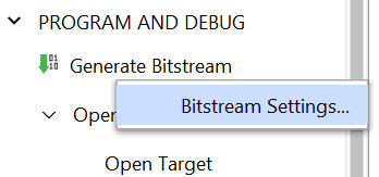
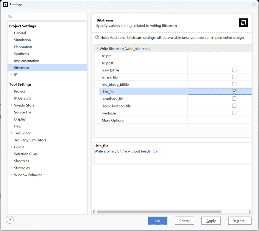
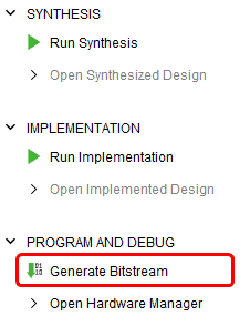
Step 1: It is recommended to generate .bin file along with .bit file. Right-click on “Generate Bitstream” under the “Program and Debug” section of the Flow Navigator window and click “Bitstream Settings”.
Step 2: Select “-bin_file” option in the dialog window and click “Apply” and then “OK”.
Step 3: Finally click “Generate Bitstream”.
Programming TityraCore Module Using USB-JTAG
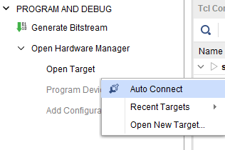
1. Ensure that Switch PGM_SEL is set to USB and Connect the USB Type-C cable to the FPGA board.
2. Click on “Auto connect” under hardware manager and it will automatically establish the connection.

Programming TityraCore Module Using JTAG
TityraCore Z7 SoC SODIMM facilitates easy reprogramming of SRAM and onboard SPI flash through JTAG programmer like “AMD Platform cable USB”. Following steps illustrate how to program FPGA on TityraCore using JTAG.
Step 1: By using JTAG cable, connect AMD platform cable USB to the carrier of TityraCore and power it up.
Step 2: Open Vivado project and open the target by clicking on the “Open Target” in “Open Hardware Manager” in the “Program and Debug” section of the Flow Navigator window. Select “Auto Connect”.
Step 3: If the device is detected successfully, then select “Program Device” after right clicking on the target device “xc7z020_1 (1)” as shown below.
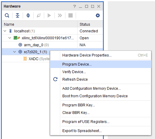
Step 4: In the dialog window which opens up, Vivado automatically chooses the correct bitstream file if the design was synthesized, implemented and bitstream generated successfully. If needed, browse to the bitstream which needs to be programmed to FPGA. Finally, click “Program”.
Programming QSPI Flash
Programming the QSPI Flash for the Zynq 7000 series is slightly different than 7-Series FPGAs. There is a tutorial on how to boot TityraCore from QSPI (as well as SD Card). Follow the same steps for TityraCore Z7 SoC module also.
Link: TityraCore: Boot from SD card and QSPI flash
Technical Specifications
Parameter * Value Unit
Basic Specifications
Number of GPIOs 126
On-board oscillator frequency 33.33 MHz
On-board oscillator frequency (ASEM1-50.000MHZ-LC-T) 50 MHz
DDR3L Capacity 2 GB
Quad SPI Flash Memory 128 Mb
Internal Processor Core Voltage 1.0 V
Auxiliary supply voltage relative to GND 1.8 V
Output drivers supply voltage relative to GND -0.5 to 3.6 V
PS MIO I/O supply voltage (VCCO_MIO) 1.8, 3.3 V
PS MIO I/O input voltage 1.8, 3.3 V
PS DDR I/O input voltage 1.35 or 1.5 V
Maximum Processor Frequency 667 MHz
* All parameters considered nominal. Numato Systems Pvt Ltd reserves the right to modify products without notice.
Mechanical Dimensions
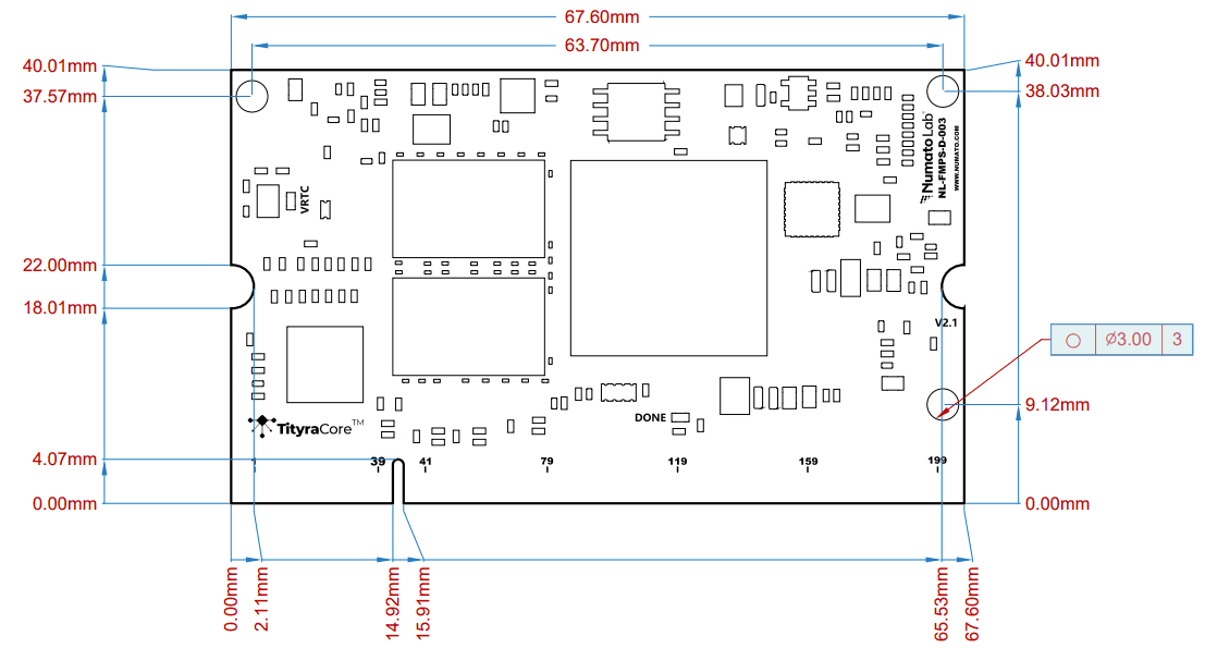
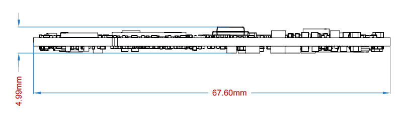
TityraCore Z7 SoC SODIMM
0 views September 24, 2024 admin 0
