Introduction
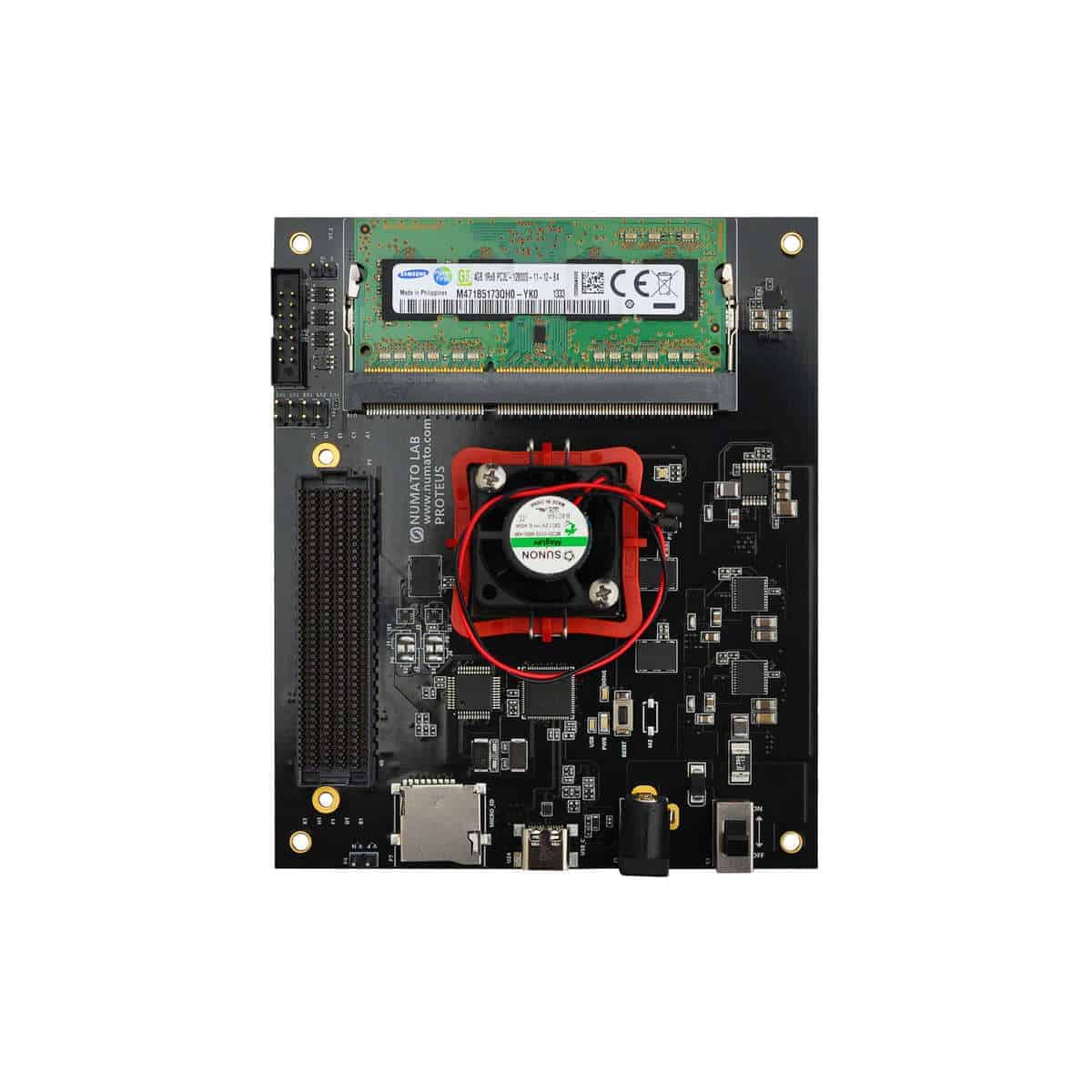
Proteus is an easy to use FPGA Development board featuring the Xilinx Kintex-7 FPGA with 4GB DDR3L SDRAM. This board contains the Xilinx XC7K160T– FBG676 FPGA. The high-speed USB 3.1 interface (USB-C connector) provides a fast and easy configuration download to the onboard SPI flash. There is no need for a programmer or special downloader cable to download bitstream to the board. The board features a High Pin Count (HPC), high-speed FMC connector for the addition of extra features to the board by utilizing a custom or commercial off-the-shelf daughter boards. Proteus provides the user the flexibility of adding their own peripherals through the ANSI/VITA 57.1 standard compliant FMC HPC connector.
Applications:
- Product Prototype Development
- Communication Devices Development
- Accelerated Computing Integration
- Development and Testing of Custom embedded processors
- Signal Processing
- Educational tool for Schools and Universities
Board Features:
- FPGA Xilinx Kintex-7 XC7K160T– FBG676 package; Speed Grade: 1
- 4GB DDR3L SODIMM SDRAM M471B5173CB0-YK0 or compatible
- 128 MB QSPI flash memory (N25Q128A13ESE40E) for Configuration and optional data storage
- 1 x 100MHz CMOS oscillator, 1x 150MHz LVDS oscillator for users
- 2 x 150MHz LVDS oscillator for GTP
- High-speed USB 3.1 interface (USB Type-C connector)
- Onboard voltage regulators for single power rail operation
- 12V DC power supply
- Maximum 130 IOs for user-defined purposes on FMC connector
- 8x GTX lanes up to 6.6Gbps on ANSI/VITA 57.1 Standard compliant FMC HPC connector
- Micro SD Card
- A push-button for the reset input
- JTAG header for programming and debugging.
- 1 RGB LED for custom use.
How to use Proteus Kintex 7 USB 3.1 Development Board
Components/Tools Required
Along with the module, you may need the accessories listed below for easy and fast installation:
- 12 V DC Power Supply.
- USB A to USB-C cable (Optional).
- A Xilinx Platform Cable USB II compatible JTAG programmer
Connection Diagram
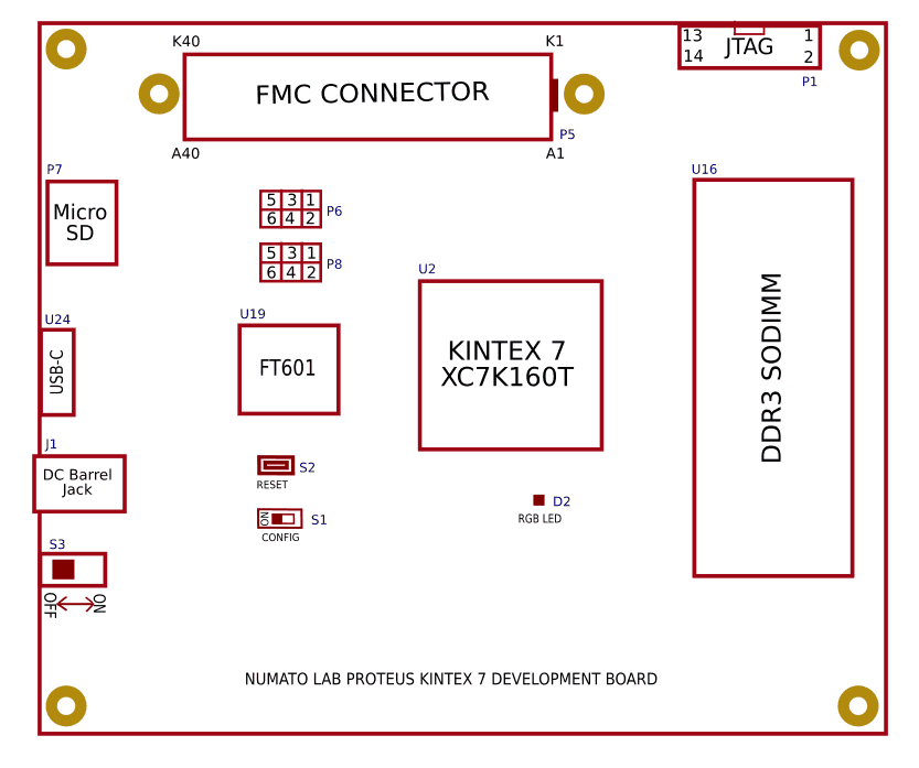
This diagram should be used as a reference only. For detailed information, see Proteus’s schematics and mechanical dimensions at the end of this page. Details of individual connectors are as shown below.
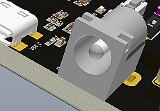
USB Interface (USB-C Connector)
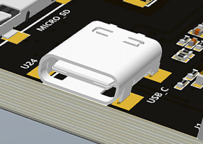 This super speed USB 3.1 interface (USB-C connector) is used to help the host PC to communicate with the module at very high speed (5Gbps). A USB-A to USB-C cable is used to connect the module to the host PC. It is primarily used to output debug information or as a console for the design running on the board. (the picture on the right shows USB-C connector).
Power
 Proteus requires a +12V power supply to function properly which can be supplied via DC Connector.
The current requirement for this board largely depends upon your application. The Proteus module works on the power supplying 0.6 A and 1 A of current for simple applications. However, a power supplying 2 A of current is recommended for a smooth running of bigger applications. Kindly consult the FPGA datasheet for more details on power requirements.
Power Switch
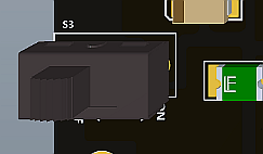 The Power Switch S3 is used to configure the power source to the board. Slide it to ON to supply power to the board from USB or External DC Jack. Slide it to OFF to power off the board.
Heat Sink
A Heat Sink comes factory-installed with Proteus to provide for heat dissipation for the Kintex-7 FPGA on board. A header is provided to optionally connect a fan (not factory installed) for forced-cooling. The fan’s speed is controlled by the FAN_PWM signal connected to FPGA IO location J25, and the signal is pulled up by default, which means unless actively driven to 0 or controlled via PWM, the fan will run at maximum speed.
SODIMM Memory Slot
Proteus features a SODIMM Memory Slot, factory-populated with 4GB DDR3L SDRAM. Only compatible modules should be inserted into this slot.
Configuration Mode Switch
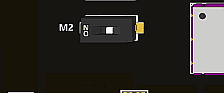 FPGA startup configuration mode can be selected using switch S1. Sliding it to ON puts FPGA in the “JTAG” configuration mode. Sliding it to OFF puts the FPGA to the “Master SPI” configuration mode.
Reset Button
Proteus features a Push-button S2 normally meant to be used as a “Reset” signal for designs running on FPGA. Push-button S2 is connected to FPGA pin C26. Push-button S2 is active-high. This pushbutton can also be used for any other input and is not just limited to be used as a Reset signal.
RGB LED
Proteus features an RGB LED which can be used for customizing or debugging purposes. The LED is wired in the active-low configuration.
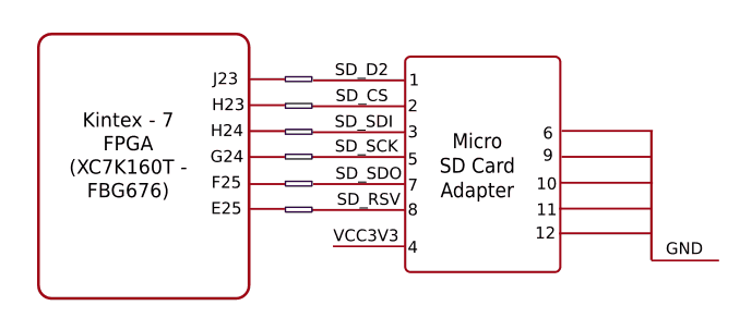
Micro SD
The Proteus board features an onboard Micro SD adapter. You can add the data logging, media storage, and other file storage by installing Micro SD Card and appropriate IP. The connection between FPGA and Micro SD Card is shown below
JTAG Chain Configuration
The Proteus FPGA JTAG chain configuration can be altered according to requirement by using the DIP switch P2 located near the JTAG Header.
Following diagram shows JTAG chain configuration: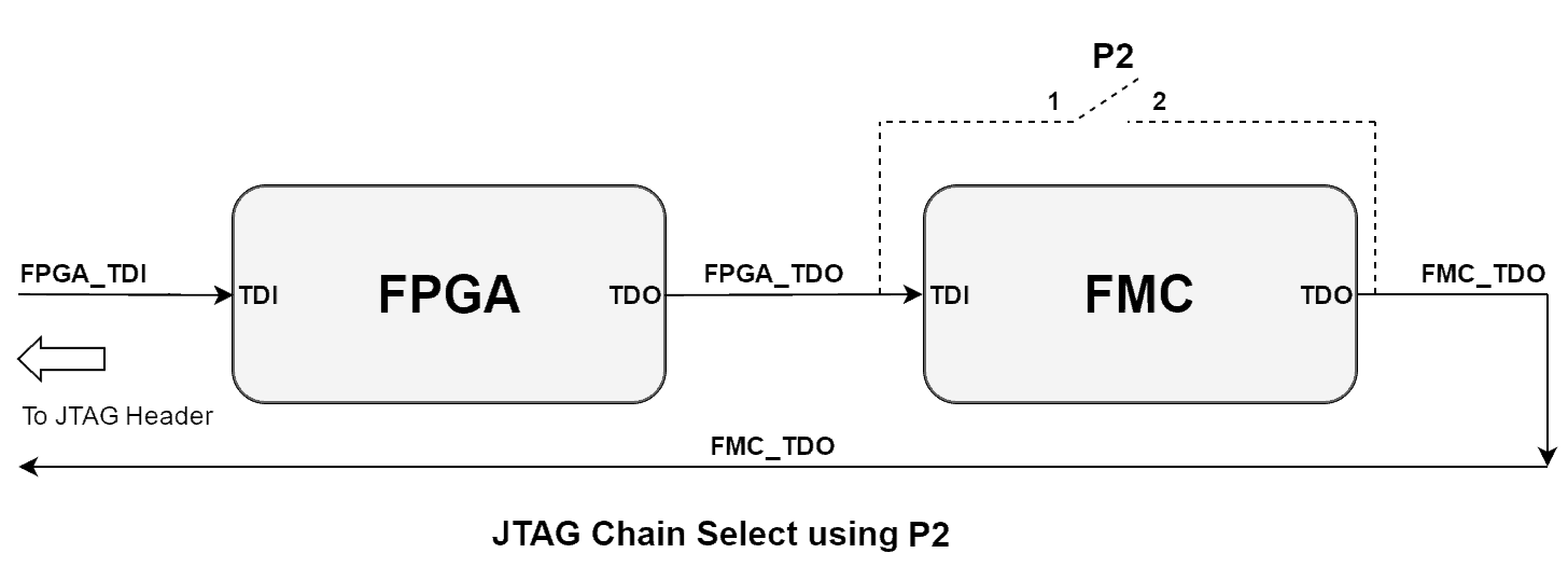
Proteus has automatic FMC detection using the PRSNT_M2C_L signal from FMC. Normally, when an FMC board is not connected, the Proteus’s onboard circuitry will automatically close the JTAG chain keeping FMC out from the chain, so no user intervention is required. But, still, jumper P2 has been provided as a redundant back up to close the JTAG chain in case the automatic circuitry doesn’t work due to non-compliant FMC modules connected to Proteus, or any or unforeseen reasons.
JTAG
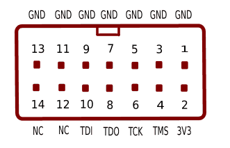
JTAG connector allows the FPGA’s JTAG registers to be accessed using a JTAG cable, compatible with Xilinx Platform Cable USB. Use this header, to attach JTAG cable for programming and debugging.
FMC VADJ Power Supply
VADJ Power Supply for FMC Bank A is configurable via jumpers J3. The following are the jumper configurations for different voltages for the VADJ supply.
| Jumper on J3 Header | FMC VADJ Power Supply (Volts) |
|---|---|
| No jumper anywhere | 3.3 |
| 1 - 2 | 2.5 |
| 3 - 4 | 1.8 |
| 5 - 6 | 1.5 |
| 7 - 8 | 1.2 |
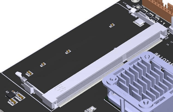
FMC Connector
Proteus features a high speed, high pin-count FMC connector which can be used to provide additional features and capabilities to it using custom or commercial-off-the-shelf daughter boards. Apart from IOs, 8 GTX lanes are available via FMC connector for custom purposes.
FMC BANKS A TO D
| A | FMC Pin Name | Kintex-7 FBG676 Pin | B | FMC Pin Name | Kintex-7 FBG676 Pin | C | FMC Pin Name | Kintex-7 FBG676 Pin | D | FMC Pin Name | Kintex-7 FBG676 Pin |
|---|---|---|---|---|---|---|---|---|---|---|---|
| A1 | GND | B1 | CLK_DIR | D23 | C1 | GND | D1 | PG_C2M | D26 | ||
| A2 | DP1_M2C_P | E4 | B2 | GND | C2 | DP0_C2M_P | F2 | D2 | GND | ||
| A3 | DP1_M2C_N | E3 | B3 | GND | C3 | DP0_C2M_N | F1 | D3 | GND | ||
| A4 | GND | B4 | DP9_M2C_P | NC | C4 | GND | D4 | GBT_CLK0_M2C_P | F6 | ||
| A5 | GND | B5 | DP9_M2C_N | NC | C5 | GND | D5 | GBT_CLK0_M2C_N | F5 | ||
| A6 | DP2_M2C_P | C4 | B6 | GND | C6 | DP0_M2C_P | G4 | D6 | GND | ||
| A7 | DP2_M2C_N | C3 | B7 | GND | C7 | DP0_M2C_N | G3 | D7 | GND | ||
| A8 | GND | B8 | DP8_M2C_P | NC | C8 | GND | D8 | LA01_CC_P | Y23 | ||
| A9 | GND | B9 | DP8_M2C_N | NC | C9 | GND | D9 | LA01_CC_N | AA24 | ||
| A10 | DP3_M2C_P | B6 | B10 | GND | C10 | LA06_P | Y25 | D10 | GND | ||
| A11 | DP3_M2C_N | B5 | B11 | GND | C11 | LA06_N | Y26 | D11 | LA05_P | W25 | |
| A12 | GND | B12 | DP7_M2C_P | J4 | C12 | GND | D12 | LA05_N | W26 | ||
| A13 | GND | B13 | DP7_M2C_N | J3 | C13 | GND | D13 | GND | |||
| A14 | DP4_M2C_P | R4 | B14 | GND | C14 | LA10_P | V21 | D14 | LA09_P | W20 | |
| A15 | DP4_M2C_N | R3 | B15 | GND | C15 | LA10_N | W21 | D15 | LA09_N | Y21 | |
| A16 | GND | B16 | DP6_M2C_P | L4 | C16 | GND | D16 | GND | |||
| A17 | GND | B17 | DP6_M2C_N | L3 | C17 | GND | D17 | LA13_P | K20 | ||
| A18 | DP5_M2C_P | N4 | B18 | GND | C18 | LA14_P | J18 | D18 | LA13_N | J20 | |
| A19 | DP5_M2C_N | N3 | B19 | GND | C19 | LA14_N | J19 | D19 | GND | ||
| A20 | GND | B20 | GBTCLK1_M2C_P | H6 | C20 | GND | D20 | LA17_CC_P | E18 | ||
| A21 | GND | B21 | GBTCLK1_M2C_N | H5 | C21 | GND | D21 | LA17_CC_N | D18 | ||
| A22 | DP1_C2M_P | D2 | B22 | GND | C22 | LA18_CC_P | F17 | D22 | GND | ||
| A23 | DP1_C2M_N | D1 | B23 | GND | C23 | LA18_CC_N | E17 | D23 | LA23_P | C17 | |
| A24 | GND | B24 | DP9_C2M_P | NC | C24 | GND | D24 | LA23_N | C18 | ||
| A25 | GND | B25 | DP9_C2M_N | NC | C25 | GND | D25 | GND | |||
| A26 | DP2_C2M_P | B2 | B26 | GND | C26 | LA27_P | G15 | D26 | LA26_P | J15 | |
| A27 | DP2_C2M_N | B1 | B27 | GND | C27 | LA27_N | F15 | D27 | LA26_N | J16 | |
| A28 | GND | B28 | DP8_C2M_P | NC | C28 | GND | D28 | GND | |||
| A29 | GND | B29 | DP8_C2M_N | NC | C29 | GND | D29 | FMC_TCK | L8 | ||
| A30 | DP3_C2M_P | A4 | B30 | GND | C30 | FMC_SCL | C21 | D30 | FPGA_TDO_FMC_TDI | R7 | |
| A31 | DP3_C2M_N | A3 | B31 | GND | C31 | FMC_SDA | B21 | D31 | TDOFMC_TDO | R6 | |
| A32 | GND | B32 | DP7_C2M_P | H2 | C32 | GND | D32 | 3V3AUX | VCC3V3 | ||
| A33 | GND | B33 | DP7_C2M_N | H1 | C33 | GND | D33 | FMC_TMS | N8 | ||
| A34 | DP4_C2M_P | P2 | B34 | GND | C34 | GND | D34 | TRST_L | NC | ||
| A35 | DP4_C2M_N | P1 | B35 | GND | C35 | 12P0V | VCC12V0 | D35 | GND | ||
| A36 | GND | B36 | DP6_C2M_P | K2 | C36 | GND | D36 | 3PV3 | VCC3V3 | ||
| A37 | GND | B37 | DP6_C2M_N | K1 | C37 | 12P0V | VCC12V0 | D37 | GND | ||
| A38 | DP5_C2M_P | M2 | B38 | GND | C38 | GND | D38 | 3PV3 | VCC3V3 | ||
| A39 | DP5_C2M_N | M1 | B39 | GND | C39 | 3PV3 | VCC3V3 | D39 | GND | ||
| A40 | GND | B40 | NC | C40 | GND | D40 | 3PV3 | VCC3V3 |
FMC BANKS E TO H
| E | FMC Pin Name | Kintex-7 FBG676 Pin | F | FMC Pin Name | Kintex-7 FBG676 Pin | G | FMC Pin Name | Kintex-7 FBG676 Pin | H | FMC Pin Name | Kintex-7 FBG676 Pin |
|---|---|---|---|---|---|---|---|---|---|---|---|
| E1 | GND | F1 | PG_M2C | E26 | G1 | GND | H1 | VREF_A_M2C | NC | ||
| E2 | HA01_CC_P | N21 | F2 | GND | G2 | CLK1_M2C_P | AC23 | H2 | PRSNT_M2C_L | B26 | |
| E3 | HA01_CC_N | N22 | F3 | GND | G3 | CLK1_M2C_N | AC24 | H3 | GND | ||
| E4 | GND | F4 | HA00_CC_P | P23 | G4 | GND | H4 | CLK0_M2C_P | Y22 | ||
| E5 | GND | F5 | HA00_CC_N | N23 | G5 | GND | H5 | CLK0_M2C_N | AA22 | ||
| E6 | HA05_P | R18 | F6 | GND | G6 | LA00_CC_P | AA23 | H6 | GND | ||
| E7 | HA05_N | P18 | F7 | HA04_P | N19 | G7 | LA00_CC_N | AB24 | H7 | LA02_P | AD26 |
| E8 | GND | F8 | HA04_N | M20 | G8 | GND | H8 | LA02_N | AE26 | ||
| E9 | HA09_P | N18 | F9 | GND | G9 | LA03_P | AA25 | H9 | GND | ||
| E10 | HA09_N | M19 | F10 | HA08_P | U19 | G10 | LA03_N | AB25 | H10 | LA04_P | AD25 |
| E11 | GND | F11 | HA08_N | U20 | G11 | GND | H11 | LA04_N | AE25 | ||
| E12 | HA13_P | U24 | F12 | GND | G12 | LA08_P | U26 | H12 | GND | ||
| E13 | HA13_N | U25 | F13 | HA12_P | T24 | G13 | LA08_N | V26 | H13 | LA07_P | V23 |
| E14 | GND | F14 | HA12_N | T25 | G14 | GND | H14 | LA07_N | V24 | ||
| E15 | HA16_P | R25 | F15 | GND | G15 | LA12_P | M17 | H15 | GND | ||
| E16 | HA16_N | P25 | F16 | HA15_P | P24 | G16 | LA12_N | L18 | H16 | LA11_P | L19 |
| E17 | GND | F17 | HA15_N | N24 | G17 | GND | H17 | LA11_N | L20 | ||
| E18 | HA20_P | M25 | F18 | GND | G18 | LA16_P | T18 | H18 | GND | ||
| E19 | HA20_N | L25 | F19 | HA19_P | K25 | G19 | LA16_N | T19 | H19 | LA15_P | U17 |
| E20 | GND | F20 | HA19_N | K26 | G20 | GND | H20 | LA15_N | T17 | ||
| E21 | HB03_P | NC | F21 | GND | G21 | LA20_P | K16 | H21 | GND | ||
| E22 | HB03_N | NC | F22 | HB02_P | NC | G22 | LA20_N | K17 | H22 | LA19_P | H16 |
| E23 | GND | F23 | HB02_N | NC | G23 | GND | H23 | LA19_N | G16 | ||
| E24 | HB05_P | NC | F24 | GND | G24 | LA22_P | C19 | H24 | GND | ||
| E25 | HB05_N | NC | F25 | HB04_P | NC | G25 | LA22_N | B19 | H25 | LA21_P | D19 |
| E26 | GND | F26 | HB04_N | NC | G26 | GND | H26 | LA21_N | D20 | ||
| E27 | HB09_P | NC | F27 | GND | G27 | LA25_P | F19 | H27 | GND | ||
| E28 | HB09_N | NC | F28 | HB08_P | NC | G28 | LA25_N | E20 | H28 | LA24_P | D15 |
| E29 | GND | F29 | HB08_N | NC | G29 | GND | H29 | LA24_N | D16 | ||
| E30 | HB13_P | NC | F30 | GND | G30 | LA29_P | E15 | H30 | GND | ||
| E31 | HB13_N | NC | F31 | HB12_P | NC | G31 | LA29_N | E16 | H31 | LA28_P | G17 |
| E32 | GND | F32 | HB12_N | NC | G32 | GND | H32 | LA28_N | F18 | ||
| E33 | HB19_P | NC | F33 | GND | G33 | LA31_P | G19 | H33 | GND | ||
| E34 | HB19_N | NC | F34 | HB16_P | NC | G34 | LA31_N | F20 | H34 | LA30_P | H17 |
| E35 | GND | F35 | HB16_N | NC | G35 | GND | H35 | LA30_N | H18 | ||
| E36 | HB21_P | NC | F36 | GND | G36 | LA33_P | L17 | H36 | GND | ||
| E37 | HB21_N | NC | F37 | HB20_P | NC | G37 | LA33_N | K18 | H37 | LA32_P | H19 |
| E38 | GND | F38 | HB20_N | NC | G38 | GND | H38 | LA32_N | G20 | ||
| E39 | VADJ | VCCVADJ | F39 | GND | G39 | VADJ | VCCVADJ | H39 | GND | ||
| E40 | GND | F40 | VADJ | VCCVADJ | G40 | GND | H40 | VADJ | VCCVADJ |
FMC BANKS J – K
| J | FMC Pin Name | Kintex-7 FBG676 Pin | K | FMC Pin Name | Kintex-7 FBG676 Pin |
|---|---|---|---|---|---|
| J1 | GND | GND | K1 | VREF_B_M2C | NC |
| J2 | CLK3_BIDIR_P | R21 | K2 | GND | GND |
| J3 | CLK3_BIDIR_N | P21 | K3 | GND | GND |
| J4 | GND | GND | K4 | CLK2_BIDIR_P | R22 |
| J5 | GND | GND | K5 | CLK2_BIDIR_N | R23 |
| J6 | HA03_P | AD23 | K6 | GND | GND |
| J7 | HA03_N | AD24 | K7 | HA02_P | AB22 |
| J8 | GND | GND | K8 | HA02_N | AC22 |
| J9 | HA07_P | R16 | K9 | GND | GND |
| J10 | HA07_N | R17 | K10 | HA06_P | P16 |
| J11 | GND | GND | K11 | HA06_N | N17 |
| J12 | HA11_P | P19 | K12 | GND | GND |
| J13 | HA11_N | P20 | K13 | HA10_P | T20 |
| J14 | GND | GND | K14 | HA10_N | R20 |
| J15 | HA14_P | R26 | K15 | GND | GND |
| J16 | HA14_N | P26 | K16 | HA17_CC_P | M21 |
| J17 | GND | GND | K17 | HA17_CC_N | M22 |
| J18 | HA18_P | N26 | K18 | GND | GND |
| J19 | HA18_N | M26 | K19 | HA21_P | M24 |
| J20 | GND | GND | K20 | HA21_N | L24 |
| J21 | HA22_P | T22 | K21 | GND | GND |
| J22 | HA22_N | T23 | K22 | HA23_P | U22 |
| J23 | GND | GND | K23 | HA23_N | V22 |
| J24 | HB01_P | NC | K24 | GND | GND |
| J25 | HB01_N | NC | K25 | HB00_CC_P | NC |
| J26 | GND | GND | K26 | HB00_CC_N | NC |
| J27 | HB07_P | NC | K27 | GND | GND |
| J28 | HB07_N | NC | K28 | HB06_CC_P | NC |
| J29 | GND | GND | K29 | HB06_CC_N | NC |
| J30 | HB11_P | NC | K30 | GND | GND |
| J31 | HB11_N | NC | K31 | HB10_P | NC |
| J32 | GND | GND | K32 | HB10_N | NC |
| J33 | HB15_P | NC | K33 | GND | GND |
| J34 | HB15_N | NC | K34 | HB14_P | NC |
| J35 | GND | GND | K35 | HB14_N | NC |
| J36 | HB18_P | NC | K36 | GND | GND |
| J37 | HB18_N | NC | K37 | HB17_CC_P | NC |
| J38 | GND | GND | K38 | HB17_CC_N | NC |
| J39 | VIO_B_M2C | NC | K39 | GND | GND |
| J40 | GND | GND | K40 | VIO_B_M2C | NC |
FT601 - Kintex-7 (FBG676) FPGA Connection Details
| FTDI Pin No. | Pin Function (245 FIFO) | Kintex-7 (FBG676) Pin No. |
|---|---|---|
| 40 | FT_D0 | J8 |
| 41 | FT_D1 | H8 |
| 42 | FT_D2 | F8 |
| 43 | FT_D3 | D8 |
| 44 | FT_D4 | A8 |
| 45 | FT_D5 | H9 |
| 46 | FT_D6 | G9 |
| 47 | FT_D7 | C9 |
| 50 | FT_D8 | B9 |
| 51 | FT_D9 | A9 |
| 52 | FT_D10 | J10 |
| 53 | FT_D11 | G10 |
| 54 | FT_D12 | F10 |
| 55 | FT_D13 | B10 |
| 56 | FT_D14 | A10 |
| 57 | FT_D15 | J11 |
| 60 | FT_D16 | H11 |
| 61 | FT_D17 | G11 |
| 62 | FT_D18 | E11 |
| 63 | FT_D19 | C11 |
| 64 | FT_D20 | B11 |
| 65 | FT_D21 | H12 |
| 66 | FT_D22 | G12 |
| 67 | FT_D23 | C12 |
| 69 | FT_D24 | B12 |
| 70 | FT_D25 | A12 |
| 71 | FT_D26 | E12 |
| 72 | FT_D27 | J13 |
| 73 | FT_D28 | H13 |
| 74 | FT_D29 | D13 |
| 75 | FT_D30 | C13 |
| 76 | FT_D31 | A13 |
| 4 | FT_BE0 | J14 |
| 5 | FT_BE1 | H14 |
| 6 | FT_BE2 | G14 |
| 7 | FT_BE3 | F14 |
| 8 | FT_TXE | D14 |
| 9 | FT_RXE | A14 |
| 11 | FT_WR | B14 |
| 12 | FT_RD | C14 |
| 13 | FT_OE | A15 |
| 15 | FT_RST | D10 |
| 16 | FT_WK | B15 |
| 58 | FT_CLK | E10 |
Driver Installation
This product requires a driver to be installed for proper functioning when used with Windows. The D3XX driver can be downloaded from http://www.ftdichip.com/Drivers/D3XX.htm. Proteus also has one FT232h which requires D2XX driver (It can be downloaded from http://www.ftdichip.com/Drivers/D2XX.htm). Windows users should download and run the latest WHQL Certified executable file that will prompt them to install the FTDI CDM drivers. When the driver installation is complete, the module should appear in Proteus Flash Config Tool as Proteus Kintex 7 USB 3.1 Development Board.
Generating Bitstream Using Vivado
The bitstream can be generated for Proteus in Vivado by following the steps below:
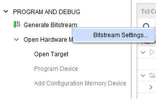
Step 1: It is recommended to generate a .bin bitstream file along with .bit bitstream file. Click “Bitstream Settings”.
Step 2: In the window that pops up, select the “-bin_file*” option and click OK.
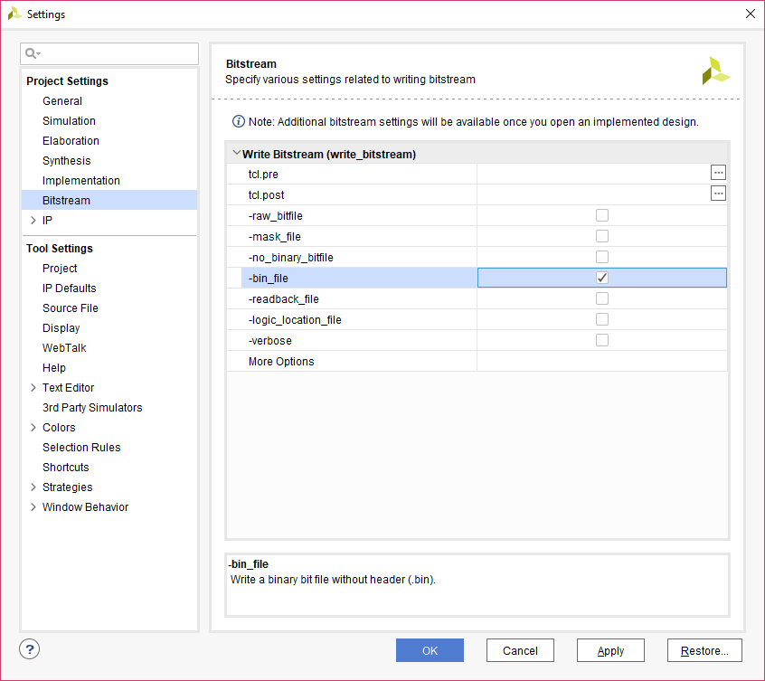
Step 3: Finally click “Generate Bitstream”.
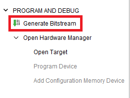
Programming Proteus Using JTAG
Proteus Kintex-7 USB 3.1 Development Board features an onboard JTAG connector that facilitates easy reprogramming of SRAM and onboard SPI flash through JTAG programmer like “Xilinx Platform cable USB”. The following steps illustrate how to program FPGA on Proteus using JTAG.
Step 1: Connect Xilinx Platform cable USB to Proteus using JTAG cable. Power up Proteus.
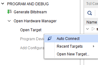
Step 2: Open Vivado Project. Click on “Open Target” in “Open Hardware Manager” in the “Program and Debug” section of the Flow Navigator window. Select “Auto Connect”.
Step 3: If the device is successfully detected, then right-click on the “xc7k160t_0(1)”. Select “Program Device” as shown below.
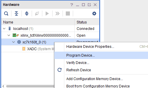
Step 4: In the dialog window which opens up, Vivado automatically chooses the correct bitstream file if the design was synthesized and implemented, and its bitstream was generated successfully. If needed, you can browse to the bitstream which needs to be programmed to the FPGA.
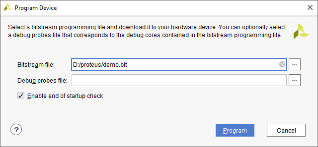
Click on the “Program” button and let the FPGA be programmed. There is a green colored LED (D1) on Proteus which was lights up as an indicator that the FPGA is not programmed. Hence, once the programming process of FPGA is completed, the LED stops glowing.
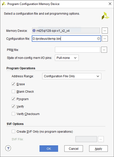
Programming QSPI Flash using Vivado
A .bin or .mcs file is required for programming Proteus’s onboard QSPI flash.
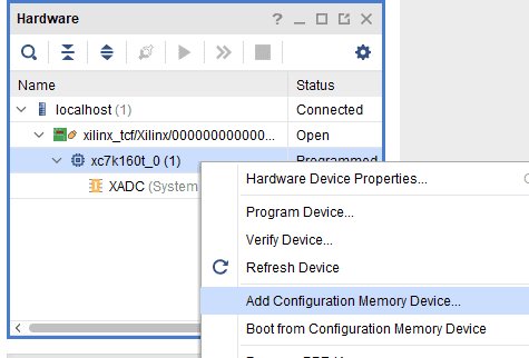
Step 1: Open Vivado Project. Click on “Open Target” in “Open Hardware Manager” in the “Program and Debug” section of the Flow Navigator window.
Step 2: If the device is successfully detected, then right-click on the “xc7k160t_0”. Select “Add Configuration Memory Device” as shown below.
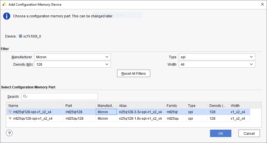
Step 3: Select the memory device “mt25ql128-spi-x1_x2_x4 (which is equivalent to n25q128-3.3v-spi-x1_x2_x4)”, then click OK.
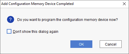
Step 4: After completion of Step 3 the following dialog box will open. Click OK.
Step 5: Browse to the working .bin file or the .mcs file (whichever applicable) and click OK to program as shown below. If programming is successful, a confirmation message will be displayed.
Technical Specifications
| Parameter* | Value | Unit |
|---|---|---|
| Basic Specifications | ||
| Number of GPIO(max) | 130 | |
| On-board Oscillator Frequency (ASEM1-100.000MHZ-LC-T) | 100 | MHz |
| On-board Oscillator Frequency (ASVMPLV-150.000MHZ-L-T) | 150 (x3) | MHz |
| DDR3 (M471B5173CB0-YK0) | 4 (x1) | Gb |
| Quad SPI Flash Memory (N25Q128A13EF840E) | 128 | Mb |
| Power Supply voltage (External) | 5 - 12 | V |
| FPGA Specifications | ||
| Internal supply voltage relative to GND | -0.5 to 1.1 | V |
| Auxillary supply voltage relative to GND | -0.5 to 2.0 | V |
| Output driver supply voltage relative to GND | -0.5 to 3.6 | |
| Connector Header (populated on Proteus) Specifications (0459714515) | ||
| Number of Positions | 400 | |
| Number of Rows | 10 | |
| Height above Board | 8.05 | mm |
| Pitch | 1.27 | mm |
| Mated Stacking Height | 10, 10.5, 11, 11.5, 12.5, 13, 15 | mm |
| Mating Connector for FMC Daughter module | 0459704715 |
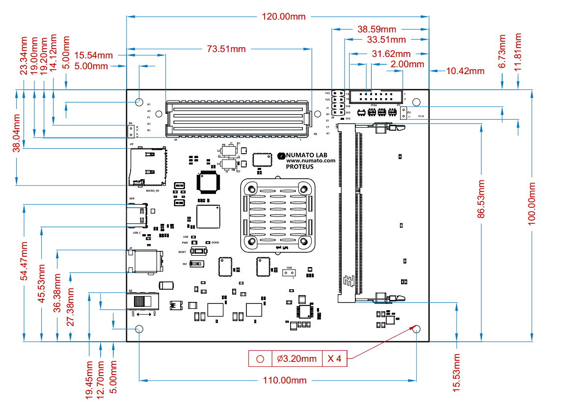
Mechanical Dimensions