Introduction
Introducing the Mimas S7 Lite FPGA Development Board: Unleash Your Creativity with Compact Power.
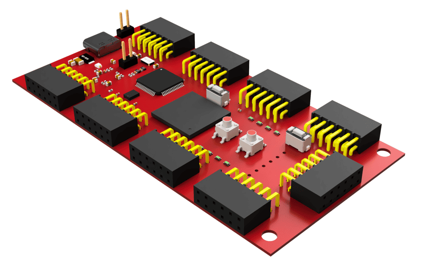
Mimas S7 Lite is an easy to use FPGA Development board featuring Spartan 7 FPGA (XC7S50 – 1CSG324C package). Ideal for diverse applications, this compact board includes QSPI flash for efficient data storage, FTDI FT2232H, 8 LEDs, 2 buttons for user interaction, and nine 6×2 headers for extensive connectivity. Whether you’re into digital signal processing, prototyping, or educational projects, the Mimas S7 Lite offers a powerful and user-friendly platform to bring your ideas to life.
Board Features
- FPGA: XC7S50 in CSGA324 package, Speed Grade: -1.
- Flash memory: 128 Mb Quadbit SPI flash memory (MT25QL128ABA1ESE-0SIT).
- 100MHz CMOS Oscillator.
- FTDI FT2232H based host interface.
- FPGA configuration via JTAG and USB (USB programming only in windows).
- 2 push buttons and 8 LEDs for User defined purposes.
- Nine PMODs for User defined purposes.
Applications
- Educational tool for Schools and Universities
- Product Prototype Development
- Accelerated computing integration
- Development and testing of custom embedded processors
- Signal Processing
- Communication devices development
- Video processing
Wiring Diagram
The following connection diagram should be used for reference only.
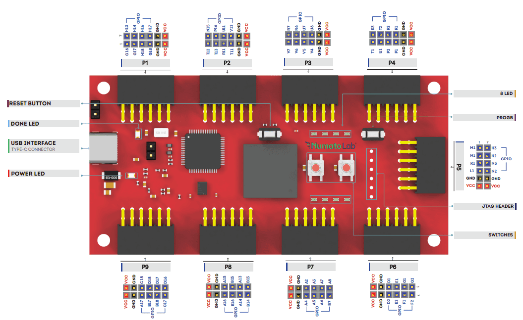
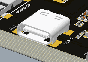
USB Interface
The onboard high speed USB controller helps a PC/Linux/Mac computer to communicate with this module. Use a USB A to C cable to connect with a PC. By default, the module is powered by USB so make sure not to overcrowd unpowered USB hubs (the picture on the right shows C connector).
Note: Mimas S7 lite ships with FT2232H Channel A dedicated to JTAG Programming.
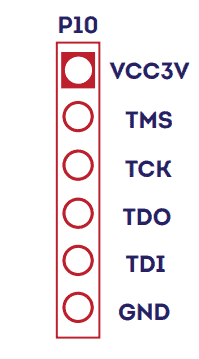
JTAG Connector
PROG_B and Reset Buttons
Mimas S7 Lite features a Push-button S1 normally meant to be used as a “PROG_B” signal for configuration reset. Push-button S1 is connected to FPGA pin R8. For enabling manual configuration reset, push-button S1 is connected to GND. The user can reconfigure the FPGA manually, by pressing this push-button S1.
“PROG_B” controls the configuration logic. When the PROG_B pin is de-asserted, resets the FPGA and initializes the new configuration.
Mimas S7 Lite features a Push-button S2 normally meant to be used as “Reset” signal for designs running on FPGA. Push-button S2 is connected to FPGA pin T14. Push-button S2 is active-high. This push button can also be used for any other input and is not just limited to be used as a Reset signal.
8 LED'S and 2 BTN's Connection

FT2232H - Spartan-7 (CSGA324) FPGA Connection Details
Pin Function (245 FIFO) Pin description Spartan 7 (CSGA324) Pin No.
FTDI-D0/TXD IO_0_14 L13
FTDI-D1/RXD IO_L6N_T0_D08_VREF_14 N13
FTDI-D2 IO_L4P_T0_D04_14 L17
FTDI-D3 IO_L4N_T0_D05_14 L18
FTDI-D4 IO_L7N_T1_D10_14 M17
FTDI-D5 IO_L8P_T1_D11_14 M18
FTDI-D6 IO_L7P_T1_D09_14 M16
FTDI-D7 IO_L8N_T1_D12_14 N18
FTDI-RXF# IO_L9N_T1_DQS_D13_14 P18
FTDI-TXE# IO_L9P_T1_DQS_14 P17
FTDI-RD# IO_L10P_T1_D14_14 R18
FTDI-WR# IO_L10N_T1_D15_14 T18
FTDI-SIWUA IO_L3N_T0_DQS_EMCCLK_14 L16
PMOD HEADERS
P1
Pin No. On The Header PMOD Pin Name FPGA PIN Pin description Pin No. On The Header PMOD Pin Name FPGA PIN Pin description
6 VCC 12 VCC
5 GND 11 GND
4 P1_2_N G18 IO_L21N_T3_DQS_15 10 P1_4_N H17 IO_L22N_T3_15
3 P1_2_P H18 IO_L21P_T3_DQS_15 9 P1_4_P H16 IO_L22P_T3_15
2 P1_1_N G17 IO_L14N_T2_SRCC_15 8 P1_3_N H14 IO_L20N_T3_15
1 P1_1_P G16 IO_L14P_T2_SRCC_15 7 P1_3_P H13 IO_L20P_T3_15
P2
Pin No. On The Header PMOD Pin Name FPGA PIN Pin description Pin No. On The Header PMOD Pin Name FPGA PIN Pin description
6 VCC 12 VCC
5 GND 11 GND
4 P2_2_N T11 IO_L23N_T3_D18_14 10 P2_4_N V12 IO_L24N_T3_D16_14
3 P2_2_P R11 IO_L23P_T3_D19_14 9 P2_4_P U11 IO_L24P_T3_D17_14
2 P2_1_N T13 IO_L22N_T3_D20_14 8 P2_3_N P16 IO_L12N_T1_MRCC_14
1 P2_1_P T12 IO_L22P_T3_D21_14 7 P2_3_P N15 IO_L12P_T1_MRCC_14
P3
Pin No. On The Header PMOD Pin Name FPGA PIN Pin description Pin No. On The Header PMOD Pin Name FPGA PIN Pin description
6 VCC 12 VCC
5 GND 11 GND
4 P3_2_N V4 IO_L17N_T2_34 10 P3_4_N U6 IO_L24N_T3_34
3 P3_2_P V5 IO_L17P_T2_34 9 P3_4_P U7 IO_L24P_T3_34
2 P3_1_N V6 IO_L20N_T3_34 8 P3_3_N R6 IO_L23N_T3_34
1 P3_1_P V7 IO_L20P_T3_34 7 P3_3_P R7 IO_L23P_T3_34
P4
Pin No. On The Header PMOD Pin Name FPGA PIN Pin description Pin No. On The Header PMOD Pin Name FPGA PIN Pin description
6 VCC 12 VCC
5 GND 11 GND
4 P4_2_N P1 IO_L11N_T1_SRCC_34 10 P4_4_N R1 IO_L12N_T1_MRCC_34
3 P4_2_P P2 IO_L11P_T1_SRCC_34 9 P4_4_P R2 IO_L12P_T1_MRCC_34
2 P4_1_N U1 IO_L14N_T2_SRCC_34 8 P4_3_N T2 IO_L13N_T2_MRCC_34
1 P4_1_P T1 IO_L14P_T2_SRCC_34 7 P4_3_P R3 IO_L13P_T2_MRCC_34
P5
Pin No. On The Header PMOD Pin Name FPGA PIN Pin description Pin No. On The Header PMOD Pin Name FPGA PIN Pin description
6 VCC 12 VCC
5 GND 11 GND
4 P5_2_N L1 IO_L3N_T0_DQS_34 10 P5_4_N N2 IO_L9N_T1_DQS_34
3 P5_2_P K1 IO_L3P_T0_DQS_34 9 P5_4_P N3 IO_L9P_T1_DQS_34
2 P5_1_N N1 IO_L8N_T1_34 8 P5_3_N K2 IO_L2N_T0_34
1 P5_1_P M1 IO_L8P_T1_34 7 P5_3_P K3 IO_L2P_T0_34
P6
Pin No. On The Header PMOD Pin Name FPGA PIN Pin description Pin No. On The Header PMOD Pin Name FPGA PIN Pin description
6 VCC 12 VCC
5 GND 11 GND
4 P6_2_N D1 IO_L14N_T2_SRCC_35 10 P6_4_N D2 IO_L16N_T2_35
3 P6_2_P E1 IO_L14P_T2_SRCC_35 9 P6_4_P E2 IO_L16P_T2_35
2 P6_1_N G1 IO_L21N_T3_DQS_35 8 P6_3_N F1 IO_L18N_T2_35
1 P6_1_P G2 IO_L21P_T3_DQS_35 7 P6_3_P F2 IO_L18P_T2_35
P7
Pin No. On The Header PMOD Pin Name FPGA PIN Pin description Pin No. On The Header PMOD Pin Name FPGA PIN Pin description
6 VCC 12 VCC
5 GND 11 GND
4 P7_2_N A2 IO_L10N_T1_AD15N_35 10 P7_4_N A4 IO_L9N_T1_DQS_AD7N_35
3 P7_2_P A3 IO_L10P_T1_AD15P_35 9 P7_4_P A5 IO_L9P_T1_DQS_AD7P_35
2 P7_1_N A7 IO_L1N_T0_AD4N_35 8 P7_3_N A6 IO_L4N_T0_35
1 P7_1_P A8 IO_L1P_T0_AD4P_35 7 P7_3_P B7 IO_L4P_T0_35
P8
Pin No. On The Header PMOD Pin Name FPGA PIN Pin description Pin No. On The Header PMOD Pin Name FPGA PIN Pin description
6 VCC 12 VCC
5 GND 11 GND
4 P8_2_N A15 IO_L3N_T0_DQS_AD1N_15 10 P8_4_N A16 IO_L4N_T0_15
3 P8_2_P B15 IO_L3P_T0_DQS_AD1P_15 9 P8_4_P B16 IO_L4P_T0_15
2 P8_1_N A13 IO_L1N_T0_AD0N_15 8 P8_3_N A14 IO_L2N_T0_AD8N_15
1 P8_1_P B13 IO_L1P_T0_AD0P_15 7 P8_3_P B14 IO_L2P_T0_AD8P_15
P9
Pin No. On The Header PMOD Pin Name FPGA PIN Pin description Pin No. On The Header PMOD Pin Name FPGA PIN Pin description
6 VCC 12 VCC
5 GND 11 GND
4 P9_2_N C18 IO_L11N_T1_SRCC_15 10 P9_4_N A17 IO_L7N_T1_AD2N_15
3 P9_2_P D18 IO_L11P_T1_SRCC_15 9 P9_4_P B17 IO_L7P_T1_AD2P_15
2 P9_1_N D17 IO_L9N_T1_DQS_AD3N_15 8 P9_3_N B18 IO_L8N_T1_AD10N_15
1 P9_1_P D16 IO_L9P_T1_DQS_AD3P_15 7 P9_3_P C17 IO_L8P_T1_AD10P_15
Generating Bitstream Using Vivado
The bitstream can be generated for Mimas S7 lite in Vivado by following the steps below:
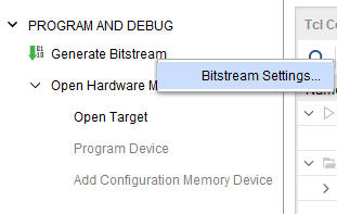
Step 1: It is recommended to generate .bin bitstream file along with .bit bitstream file. Click “Bitstream Settings”.
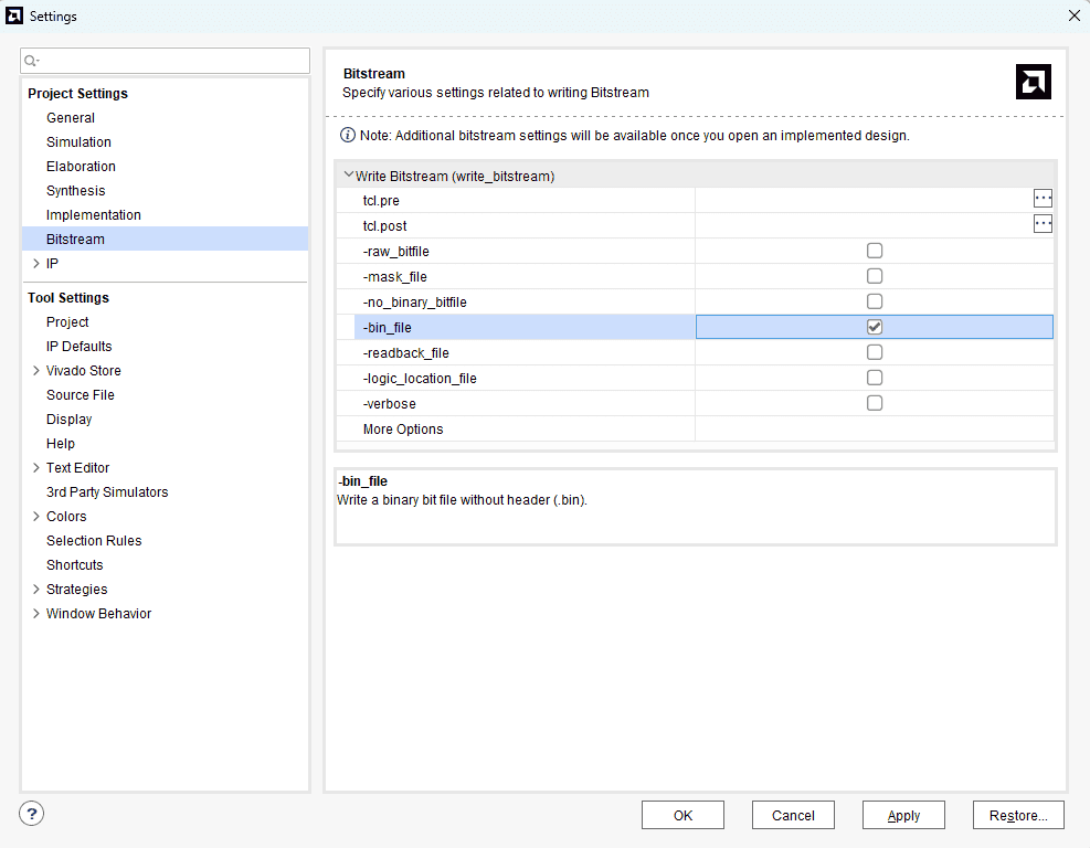
Step 2: Select “-bin_file*” option in the dialog window and Click OK.
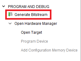
Step 3: Finally click “Generate Bitstream”.
Programming Mimas S7 lite Using JTAG
For JTAG programming remove the jumper from header P13.
Mimas Spartan7 Lite FPGA features an onboard JTAG connector which facilitates easy reprogramming of SRAM and onboard SPI flash through JTAG programmer like “Xilinx Platform cable USB”. Following steps illustrate how to program FPGA on Mimas S7 Lite using JTAG.
Step 1: By using JTAG cable, connect Xilinx platform cable USB to Mimas S7 Lite and power it up.
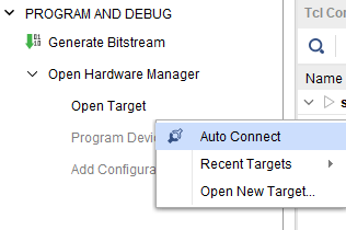
Step 2: Open Vivado project and open the target by clicking on the “Open Target” in “Open Hardware Manager” in the “Program and Debug” section of the Flow Navigator window. Select “Auto Connect”.
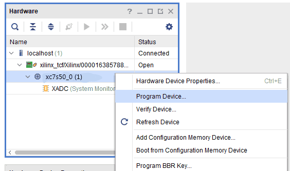
Step 3: If the device is detected successfully, then select “Program Device” after right clicking on the target device “XC7S50_0” as shown below.
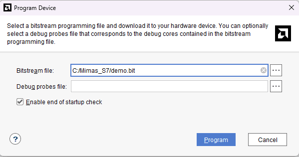
Step 4: In the dialog window which opens up, Vivado automatically chooses correct bitstream file if the design was synthesized, implemented and bitstream generated successfully. If needed, browse to the bitstream which needs to be programmed to FPGA. Finally, click “Program”.
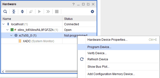
As soon as “Program” is clicked, a green colored DONE LED (D1) on Mimas S7 should light up, indicating that programming process is going on. This LED will turn off when the configuration is complete.
Programming Mimas S7 lite Using USB-JTAG
1. Ensure that header P13 is populated with a jumper and Connect the USB Type-C cable to the FPGA board.
2. Click on “Auto connect” under hardware manager and it will automatically establish the connection.
Programming QSPI Flash using Vivado
A .bin or .mcs file is required for programming Mimas S7 lite’s onboard QSPI flash.
Step 1: Open Vivado project and open the target by clicking on the “Open Target” in “Open Hardware Manager” in the “Program and Debug” section of the Flow Navigator window. Select “Auto Connect”.
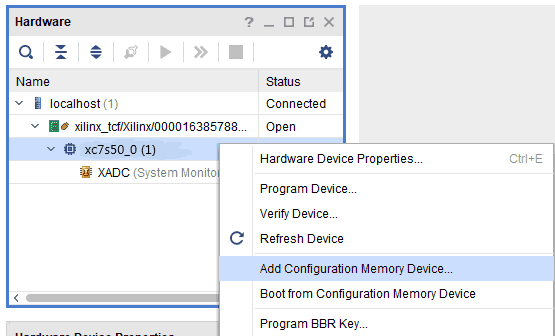
Step 2: If the device is detected successfully, then select “Add Configuration Memory Device” after right clicking on the target device “xc7s50_0” as shown below.
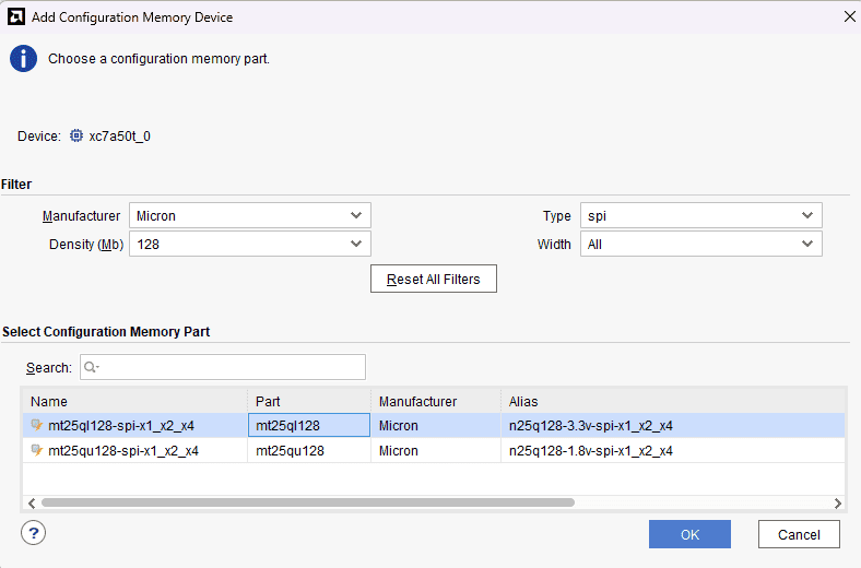
Step 3: Select the memory device “mt25ql128-spi-x1_x2_x4”, then click OK.
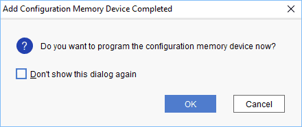
Step 4: After completion of Step 3 the following dialog box will open. Click OK.
Step 5: Browse to the working .bin file or the .mcs file (whichever applicable) and click OK to program as shown below. If programming is successful, a confirmation message will be displayed.

Technical Specifications
Parameter * Value Unit
Basic Specifications
Number of PMODs 9
On-board oscillator frequency (ASEM1-100.000MHZ-LC-T) 100 MHz
Quad SPI Flash Memory (MT25QL128ABA1ESE-0SIT) 128 Mb
USB Power supply voltage 5 V
FPGA Specifications
Internal supply voltage relative to GND -0.5 to 1.1 V
Auxiliary supply voltage relative to GND -0.5 to 2.0 V
Output drivers supply voltage relative to GND -0.5 to 3.6 V
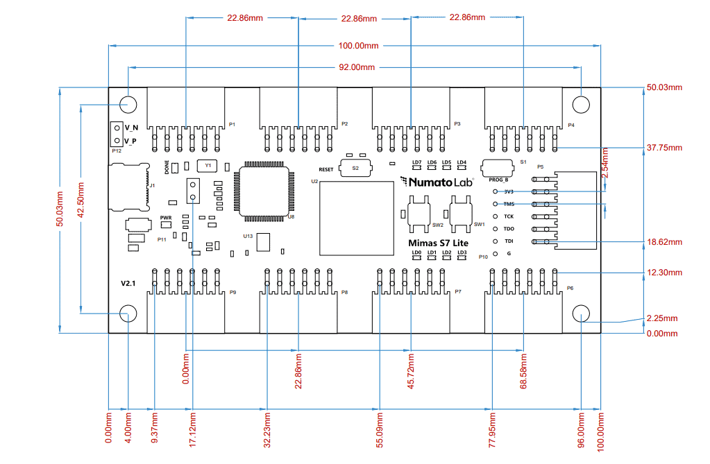
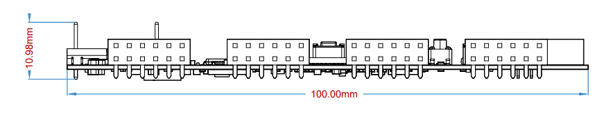
Mechanical Dimensions
Help Guide Powered by Documentor Mimas S7 Lite
0 views April 4, 2024 megha-m 0
