Introduction
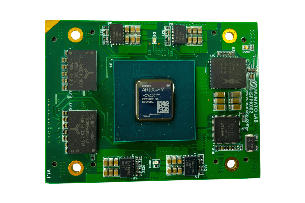
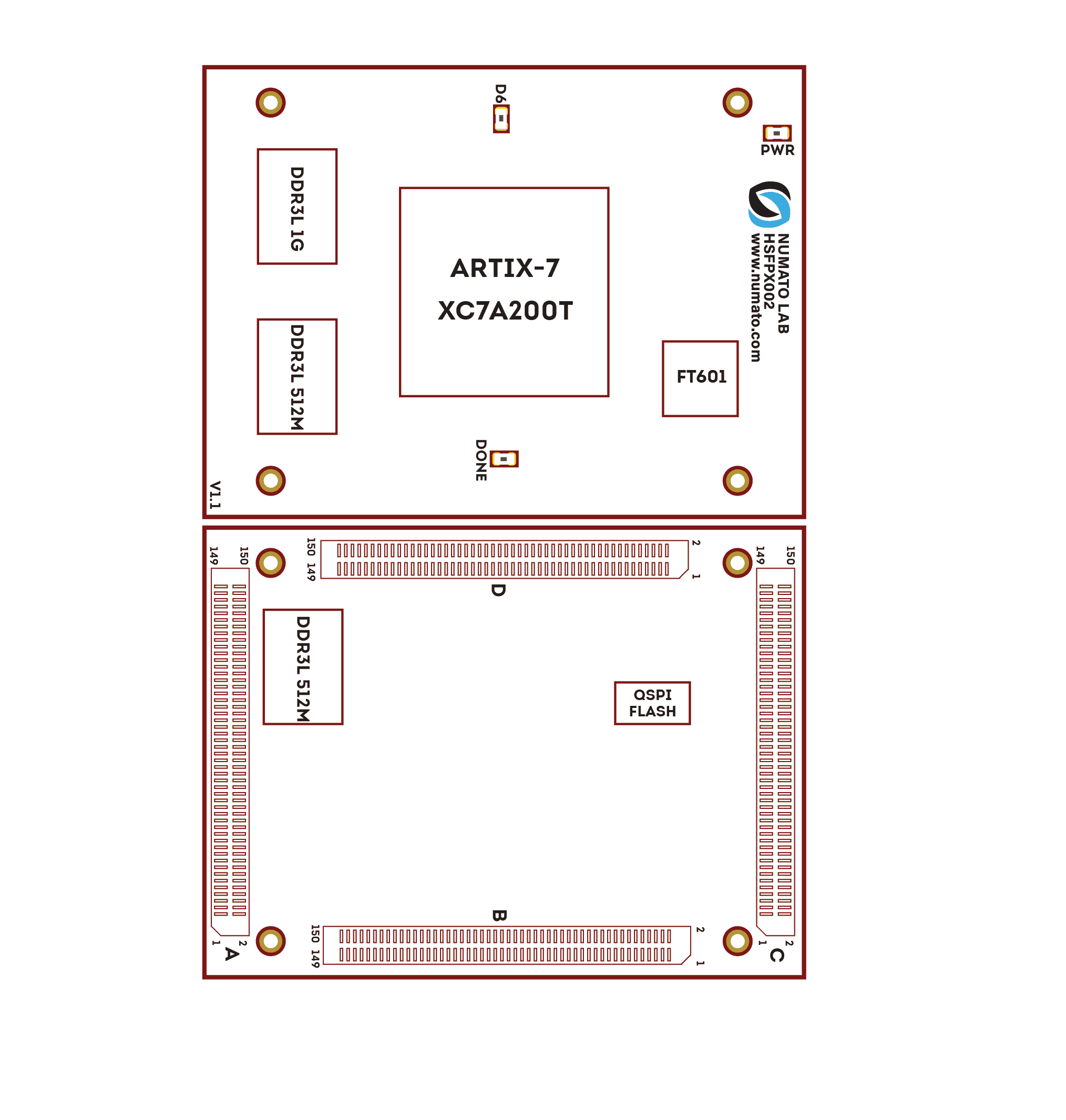
HSFPX002 is an easy to use FPGA module featuring the Xilinx Artix 7 FPGA with total size of 24Gb DDR3 SDRAM. This board contains the Xilinx XC7A200T– FBG676 FPGA. This board features an Edge Rate® Rugged High-Speed Male connector, so this board works with the carrier boards (like Numato Lab’s HSFPX00X carrier board) that feature Edge Rate® Rugged High-Speed female connectors. This board has the FT601 IC for the configuration and communication between FPGA and USB host.
Board Features
- FPGA: Artix XC7A200T in FBG676 package
- DDR3: 1x8Gb DDR3 (MT41K1G8SN-125:A) & two combined 512x16Mb DDR3 (MT41K512M16HA-125:A TR)
- Flash memory: 512 Mb Quad SPI flash memory (S25FL512SDSBHV210/IS25LP512M-RHLE)
- 1 x 100MHz CMOS oscillator
-
4x Edge Rate® Rugged High-Speed Male connectors
- 8 GTP lanes (up to 6.6 GT/s)
- FTDI FT601 for FPGA and Host communication
- Onboard voltage regulators for single-power rail operation
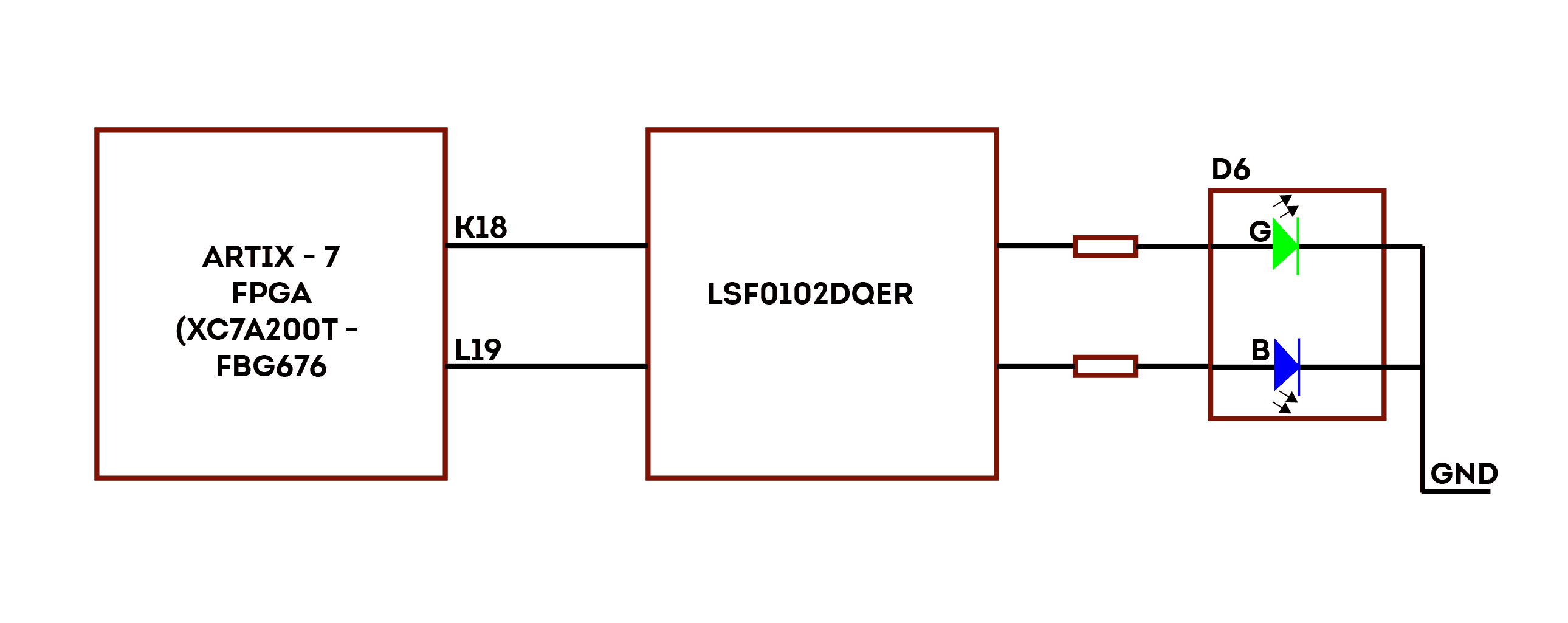
- 1 Bi-color LED for custom use
- Maximum IOs for user-defined purposes
- FPGA – 96 differential I/O pairs
Applications
- Product Prototype Development
- Accelerated computing integration
- Memory Intensive FPGA development
- Data Acquisition
- Educational tool for Schools and Universities
How to use HSFPX002 FPGA Board
The following sections describe in detail how to use this module.
Hardware Accessories Required
Along with the module, you may need the accessories listed below for easy and fast installation:
- 12 V DC Power Supply.
- USB A to USB-C cable.
- HSFPX00X Carrier Board.
- A Xilinx Platform Cable USB II compatible JTAG programmer.
Connection Diagram
This diagram should be used as a reference only. For detailed information, see HSFPX002’s schematics and mechanical dimensions at the end of this page. Details of individual connectors are as shown below.
Bi-color LED
HSFPX002 features one Bi-color LED which can be used for custom or debug purposes.
GPIOs
This device is equipped with a maximum 96 user IO pins that can be used for various custom applications. All user IOs are length matched and can be used as differential pairs.
Connector A
| PIN NO. ON CONNECTOR | GPIO PIN NAME | Artix 7 (XC7A200T-2FBG676) | PIN NO. ON CONNECTOR | GPIO PIN NAME | Artix 7 (XC7A200T-2FBG676) |
|---|---|---|---|---|---|
| 1 | EXT_VIN | 2 | EXT_VIN | ||
| 3 | GND | 4 | GND | ||
| 5 | NC | 6 | NC | ||
| 7 | NC | 8 | NC | ||
| 9 | GND | 10 | GND | ||
| 11 | NC | 12 | NC | ||
| 13 | NC | 14 | NC | ||
| 15 | GND | 16 | GND | ||
| 17 | NC | 18 | NC | ||
| 19 | NC | 20 | NC | ||
| 21 | GND | 22 | GND | ||
| 23 | NC | 24 | NC | ||
| 25 | NC | 26 | NC | ||
| 27 | GND | 28 | GND | ||
| 29 | NC | 30 | NC | ||
| 31 | NC | 32 | NC | ||
| 33 | GND | 34 | GND | ||
| 35 | NC | 36 | NC | ||
| 37 | NC | 38 | NC | ||
| 39 | GND | 40 | GND | ||
| 41 | NC | 42 | NC | ||
| 43 | NC | 44 | NC | ||
| 45 | GND | 46 | GND | ||
| 47 | NC | 48 | NC | ||
| 49 | NC | 50 | NC | ||
| 51 | GND | 52 | GND | ||
| 53 | NC | 54 | NC | ||
| 55 | NC | 56 | NC | ||
| 57 | GND | 58 | GND | ||
| 59 | NC | 60 | NC | ||
| 61 | NC | 62 | NC | ||
| 63 | GND | 64 | GND | ||
| 65 | MGTAVTT | 66 | MGTAVTT | ||
| 67 | GND | 68 | GND | ||
| 69 | NC | 70 | NC | ||
| 71 | GND | 72 | GND | ||
| 73 | B216_GTP_CLK0_P | F11 | 74 | B216_GTP_CLK1_P | E11 |
| 75 | B216_GTP_CLK0_N | F13 | 76 | B216_GTP_CLK1_N | E13 |
| 77 | GND | 78 | GND | ||
| 79 | B216_GTP_RX3_P | D12 | 80 | B216_GTP_TX3_P | D10 |
| 81 | B216_GTP_RX3_N | C12 | 82 | B216_GTP_TX3_N | C10 |
| 83 | GND | 84 | GND | ||
| 85 | B216_GTP_RX2_P | B13 | 86 | B216_GTP_TX2_P | B9 |
| 87 | B216_GTP_RX2_N | A13 | 88 | B216_GTP_TX2_N | A9 |
| 89 | GND | 90 | GND | ||
| 91 | B216_GTP_RX1_P | D14 | 92 | B216_GTP_TX1_P | D8 |
| 93 | B216_GTP_RX1_N | C14 | 94 | B216_GTP_TX1_N | C8 |
| 95 | GND | 96 | GND | ||
| 97 | B216_GTP_RX0_P | B11 | 98 | B216_GTP_TX0_P | B7 |
| 99 | B216_GTP_RX0_N | A11 | 100 | B216_GTP_TX0_N | A7 |
| 101 | GND | 102 | GND | ||
| 103 | B213_GTP_CLK0_P | AA13 | 104 | B213_GTP_CLK1_P | AA11 |
| 105 | B213_GTP_CLK0_N | AB13 | 106 | B213_GTP_CLK1_N | AB11 |
| 107 | GND | 108 | GND | ||
| 109 | B213_GTP_RX3_P | AE11 | 110 | B213_GTP_TX3_P | AE7 |
| 111 | B213_GTP_RX3_N | AF11 | 112 | B213_GTP_TX3_N | AF7 |
| 113 | GND | 114 | GND | ||
| 115 | B213_GTP_RX2_P | AC14 | 116 | B213_GTP_TX2_P | AC8 |
| 117 | B213_GTP_RX2_N | AD14 | 118 | B213_GTP_TX2_N | AD8 |
| 119 | GND | 120 | GND | ||
| 121 | B213_GTP_RX1_P | AE13 | 122 | B213_GTP_TX1_P | AE9 |
| 123 | B213_GTP_RX1_N | AF13 | 124 | B213_GTP_TX1_N | AF9 |
| 125 | GND | 126 | GND | ||
| 127 | B213_GTP_RX0_P | AC12 | 128 | B213_GTP_TX0_P | AC10 |
| 129 | B213_GTP_RX0_N | AD12 | 130 | B213_GTP_TX0_N | AD10 |
| 131 | GND | 132 | GND | ||
| 133 | NC | 134 | NC | ||
| 135 | NC | 136 | NC | ||
| 137 | NC | 138 | NC | ||
| 139 | NC | 140 | NC | ||
| 141 | GND | 142 | GND | ||
| 143 | MGTAVCC | 144 | MGTAVCC | ||
| 145 | MGTAVCC | 146 | MGTAVCC | ||
| 147 | GND | 148 | GND | ||
| 149 | EXT_VIN | 150 | EXT_VIN |
Connector B
| PIN NO. ON CONNECTOR | GPIO PIN NAME | Artix 7 (XC7A200T-2FBG676) | PIN NO. ON CONNECTOR | GPIO PIN NAME | Artix 7 (XC7A200T-2FBG676) |
|---|---|---|---|---|---|
| 1 | EXT_VIN | 2 | EXT_VIN | ||
| 3 | GND | 4 | GND | ||
| 5 | B15_IO_0_P | J25 | 6 | B15_IO_2_P | K15 |
| 7 | B15_IO_0_N | J26 | 8 | B15_IO_2_N | J16 |
| 9 | B15_IO_1_P | H26 | 10 | B15_IO_3_P | K22 |
| 11 | B15_IO_1_N | G26 | 12 | B15_IO_3_N | K23 |
| 13 | GND | 14 | GND | ||
| 15 | B15_IO_4_P | E25 | 16 | B15_IO_6_P | M16 |
| 17 | B15_IO_4_N | D25 | 18 | B15_IO_6_N | M17 |
| 19 | B15_IO_5_P | G24 | 20 | B15_IO_7_P | K16 |
| 21 | B15_IO_5_N | F24 | 22 | B15_IO_7_N | K17 |
| 23 | GND | 24 | GND | ||
| 25 | B15_IO_8_P | F23 | 26 | B15_IO_10_P | L17 |
| 27 | B15_IO_8_N | E23 | 28 | B15_IO_10_N | L18 |
| 29 | B15_IO_9_P | J24 | 30 | B15_IO_11_P | K20 |
| 31 | B15_IO_9_N | H24 | 32 | B15_IO_11_N | J20 |
| 33 | GND | 34 | GND | ||
| 35 | B15_IO_12_P | J23 | 36 | B15_IO_14_P | E26 |
| 37 | B15_IO_12_N | H23 | 38 | B15_IO_14_N | D26 |
| 39 | B15_IO_13_P | K21 | 40 | B15_IO_15_P | G25 |
| 41 | B15_IO_13_N | J21 | 42 | B15_IO_15_N | F25 |
| 43 | GND | 44 | GND | ||
| 45 | B15_IO_16_P | J18 | 46 | B15_IO_18_P | G20 |
| 47 | B15_IO_16_N | H18 | 48 | B15_IO_18_N | G21 |
| 49 | B15_IO_17_P | M15 | 50 | B15_IO_19_P | J19 |
| 51 | B15_IO_17_N | L15 | 52 | B15_IO_19_N | H19 |
| 53 | GND | 54 | GND | ||
| 55 | B15_IO_20_P | M14 | 56 | B15_IO_22_P | G22 |
| 57 | B15_IO_20_N | L14 | 58 | B15_IO_22_N | F22 |
| 59 | B15_IO_21_P | J14 | 60 | B15_IO_23_P | H21 |
| 61 | B15_IO_21_N | J15 | 62 | B15_IO_23_N | H22 |
| 63 | GND | 64 | GND | ||
| 65 | B15_VADJ | 66 | B15_VADJ | ||
| 67 | GND | 68 | GND | ||
| 69 | B16_VADJ | 70 | B16_VADJ | ||
| 71 | GND | 72 | GND | ||
| 73 | B16_IO_0_P | C26 | 74 | B16_IO_2_P | B20 |
| 75 | B16_IO_0_N | B26 | 76 | B16_IO_2_N | A20 |
| 77 | B16_IO_1_P | B25 | 78 | B16_IO_3_P | G19 |
| 79 | B16_IO_1_N | A25 | 80 | B16_IO_3_N | F20 |
| 81 | GND | 82 | GND | ||
| 83 | B16_IO_4_P | C24 | 84 | B16_IO_6_P | E20 |
| 85 | B16_IO_4_N | B24 | 86 | B16_IO_6_N | D20 |
| 87 | B16_IO_5_P | A23 | 88 | B16_IO_7_P | F18 |
| 89 | B16_IO_5_N | A24 | 90 | B16_IO_7_N | F19 |
| 91 | GND | 92 | GND | ||
| 93 | B16_IO_8_P | B22 | 94 | B16_IO_10_P | G17 |
| 95 | B16_IO_8_N | A22 | 96 | B16_IO_10_N | F17 |
| 97 | B16_IO_9_P | C21 | 98 | B16_IO_11_P | D18 |
| 99 | B16_IO_9_N | B21 | 100 | B16_IO_11_N | C18 |
| 101 | GND | 102 | GND | ||
| 103 | B16_IO_12_P | C22 | 104 | B16_IO_14_P | H16 |
| 105 | B16_IO_12_N | C23 | 106 | B16_IO_14_N | G16 |
| 107 | B16_IO_13_P | D19 | 108 | B16_IO_15_P | E17 |
| 109 | B16_IO_13_N | C19 | 110 | B16_IO_15_N | E18 |
| 111 | GND | 112 | GND | ||
| 113 | B16_IO_16_P | E21 | 114 | B16_IO_18_P | G15 |
| 115 | B16_IO_16_N | D21 | 116 | B16_IO_18_N | F15 |
| 117 | B16_IO_17_P | D23 | 118 | B16_IO_19_P | E16 |
| 119 | B16_IO_17_N | D24 | 120 | B16_IO_19_N | D16 |
| 121 | GND | 122 | GND | ||
| 123 | B16_IO_20_P | B19 | 124 | B16_IO_22_P | H14 |
| 125 | B16_IO_20_N | A19 | 126 | B16_IO_22_N | H15 |
| 127 | B16_IO_21_P | A17 | 128 | B16_IO_23_P | C17 |
| 129 | B16_IO_21_N | A18 | 130 | B16_IO_23_N | B17 |
| 131 | GND | 132 | GND | ||
| 133 | TDI | H10 | 134 | TDO | J10 |
| 135 | TMS | H11 | 136 | TCK | H12 |
| 137 | VCC_BAT | 138 | V_P | N12 | |
| 139 | PROG_B | AE16 | 140 | V_N | P11 |
| 141 | GND | 142 | GND | ||
| 143 | VCC3V3 | 144 | VCC3V3 | ||
| 145 | VCC3V3 | 146 | VCC3V3 | ||
| 147 | GND | 148 | GND | ||
| 149 | EXT_VIN | 150 | EXT_VIN |
Connector C
| PIN NO. ON CONNECTOR | GPIO PIN NAME | Artix 7 (XC7A200T2FBG676) | PIN NO. ON CONNECTOR | GPIO PIN NAME | Artix 7 (XC7A200T2FBG676) |
|---|---|---|---|---|---|
| 1 | EXT_VIN | 2 | EXT_VIN | ||
| 3 | GND | 4 | GND | ||
| 5 | NC | 6 | NC | ||
| 7 | NC | 8 | NC | ||
| 9 | NC | 10 | USB_D_P | N/A (Connected to FT601) | |
| 11 | NC | 12 | USB_D_N | N/A (Connected to FT601) | |
| 13 | GND | 14 | GND | ||
| 15 | NC | 16 | USB_RX_P | N/A (Connected to FT601) | |
| 17 | NC | 18 | USB_RX_N | N/A (Connected to FT601) | |
| 19 | NC | 20 | USB_TX_P | N/A (Connected to FT601) | |
| 21 | NC | 22 | USB_TX_N | N/A (Connected to FT601) | |
| 23 | GND | 24 | GND | ||
| 25 | NC | 26 | NC | ||
| 27 | NC | 28 | NC | ||
| 29 | NC | 30 | NC | ||
| 31 | NC | 32 | NC | ||
| 33 | NC | 34 | NC | ||
| 35 | NC | 36 | NC | ||
| 37 | NC | 38 | NC | ||
| 39 | NC | 40 | NC | ||
| 41 | NC | 42 | NC | ||
| 43 | NC | 44 | NC | ||
| 45 | NC | 46 | NC | ||
| 47 | NC | 48 | NC | ||
| 49 | NC | 50 | NC | ||
| 51 | NC | 52 | NC | ||
| 53 | NC | 54 | NC | ||
| 55 | NC | 56 | NC | ||
| 57 | NC | 58 | NC | ||
| 59 | NC | 60 | NC | ||
| 61 | NC | 62 | NC | ||
| 63 | GND | 64 | GND | ||
| 65 | NC | 66 | NC | ||
| 67 | GND | 68 | GND | ||
| 69 | NC | 70 | NC | ||
| 71 | GND | 72 | GND | ||
| 73 | NC | 74 | NC | ||
| 75 | NC | 76 | NC | ||
| 77 | NC | 78 | NC | ||
| 79 | NC | 80 | NC | ||
| 81 | GND | 82 | GND | ||
| 83 | NC | 84 | NC | ||
| 85 | NC | 86 | NC | ||
| 87 | NC | 88 | NC | ||
| 89 | NC | 90 | NC | ||
| 91 | GND | 92 | GND | ||
| 93 | NC | 94 | NC | ||
| 95 | NC | 96 | NC | ||
| 97 | NC | 98 | NC | ||
| 99 | NC | 100 | NC | ||
| 101 | GND | 102 | GND | ||
| 103 | NC | 104 | NC | ||
| 105 | NC | 106 | NC | ||
| 107 | NC | 108 | NC | ||
| 109 | NC | 110 | NC | ||
| 111 | GND | 112 | GND | ||
| 113 | NC | 114 | NC | ||
| 115 | NC | 116 | NC | ||
| 117 | NC | 118 | NC | ||
| 119 | NC | 120 | NC | ||
| 121 | GND | 122 | GND | ||
| 123 | NC | 124 | NC | ||
| 125 | NC | 126 | NC | ||
| 127 | NC | 128 | NC | ||
| 129 | NC | 130 | NC | ||
| 131 | GND | 132 | GND | ||
| 133 | NC | 134 | NC | ||
| 135 | NC | 136 | NC | ||
| 137 | NC | 138 | NC | ||
| 139 | NC | 140 | NC | ||
| 141 | GND | 142 | GND | ||
| 143 | NC | 144 | NC | ||
| 145 | NC | 146 | NC | ||
| 147 | GND | 148 | GND | ||
| 149 | EXT_VIN | 150 | EXT_VIN |
Connector D
| PIN NO. ON CONNECTOR | GPIO PIN NAME | Artix 7 (XC7A200T-2FBG676) | PIN NO. ON CONNECTOR | GPIO PIN NAME | Artix 7 (XC7A200T-2FBG676) |
|---|---|---|---|---|---|
| 1 | EXT_VIN | 2 | EXT_VIN | ||
| 3 | GND | 4 | GND | ||
| 5 | B12_IO_0_P | AA20 | 6 | B12_IO_2_P | AD23 |
| 7 | B12_IO_0_N | AB20 | 8 | B12_IO_2_N | AD24 |
| 9 | B12_IO_1_P | AB21 | 10 | B12_IO_3_P | AD25 |
| 11 | B12_IO_1_N | AC21 | 12 | B12_IO_3_N | AD26 |
| 13 | GND | 14 | GND | ||
| 15 | B12_IO_4_P | AE23 | 16 | B12_IO_6_P | AE25 |
| 17 | B12_IO_4_N | AF23 | 18 | B12_IO_6_N | AE26 |
| 19 | B12_IO_5_P | AA19 | 20 | B12_IO_7_P | AC22 |
| 21 | B12_IO_5_N | AB19 | 22 | B12_IO_7_N | AC23 |
| 23 | GND | 24 | GND | ||
| 25 | B12_IO_8_P | AE17 | 26 | B12_IO_10_P | AF19 |
| 27 | B12_IO_8_N | AF17 | 28 | B12_IO_10_N | AF20 |
| 29 | B12_IO_9_P | Y18 | 30 | B12_IO_11_P | AF24 |
| 31 | B12_IO_9_N | AA18 | 32 | B12_IO_11_N | AF25 |
| 33 | GND | 34 | GND | ||
| 35 | B12_IO_12_P | Y16 | 36 | B12_IO_14_P | AE22 |
| 37 | B12_IO_12_N | Y17 | 38 | B12_IO_14_N | AF22 |
| 39 | B12_IO_13_P | AC18 | 40 | B12_IO_15_P | AD21 |
| 41 | B12_IO_13_N | AD18 | 42 | B12_IO_15_N | AE21 |
| 43 | GND | 44 | GND | ||
| 45 | B12_IO_16_P | AB16 | 46 | B12_IO_18_P | AD20 |
| 47 | B12_IO_16_N | AC16 | 48 | B12_IO_18_N | AE20 |
| 49 | B12_IO_17_P | AC17 | 50 | B12_IO_19_P | AC19 |
| 51 | B12_IO_17_N | AD17 | 52 | B12_IO_19_N | AD19 |
| 53 | GND | 54 | GND | ||
| 55 | B12_IO_20_P | Y15 | 56 | B12_IO_22_P | AE18 |
| 57 | B12_IO_20_N | AA15 | 58 | B12_IO_22_N | AF18 |
| 59 | B12_IO_21_P | W14 | 60 | B12_IO_23_P | AA17 |
| 61 | B12_IO_21_N | W15 | 62 | B12_IO_23_N | AB17 |
| 63 | GND | 64 | GND | ||
| 65 | B12_VADJ | 66 | B12_VADJ | ||
| 67 | GND | 68 | GND | ||
| 69 | B13_VADJ | 70 | B13_VADJ | ||
| 71 | GND | 72 | GND | ||
| 73 | B13_IO_0_P | AB24 | 74 | B13_IO_2_P | AB26 |
| 75 | B13_IO_0_N | AC24 | 76 | B13_IO_2_N | AC26 |
| 77 | B13_IO_1_P | T19 | 78 | B13_IO_3_P | W25 |
| 79 | B13_IO_1_N | U19 | 80 | B13_IO_3_N | Y26 |
| 81 | GND | 82 | GND | ||
| 83 | B13_IO_4_P | Y25 | 84 | B13_IO_6_P | AA24 |
| 85 | B13_IO_4_N | AA25 | 86 | B13_IO_6_N | AB25 |
| 87 | B13_IO_5_P | V19 | 88 | B13_IO_7_P | AA22 |
| 89 | B13_IO_5_N | W19 | 90 | B13_IO_7_N | AA23 |
| 91 | GND | 92 | GND | ||
| 93 | B13_IO_8_P | T17 | 94 | B13_IO_10_P | Y22 |
| 95 | B13_IO_8_N | T18 | 96 | B13_IO_10_N | Y23 |
| 97 | B13_IO_9_P | V26 | 98 | B13_IO_11_P | W20 |
| 99 | B13_IO_9_N | W26 | 100 | B13_IO_11_N | Y20 |
| 101 | GND | 102 | GND | ||
| 103 | B13_IO_12_P | U25 | 104 | B13_IO_14_P | W21 |
| 105 | B13_IO_12_N | U26 | 106 | B13_IO_14_N | Y21 |
| 107 | B13_IO_13_P | V23 | 108 | B13_IO_15_P | V18 |
| 109 | B13_IO_13_N | W23 | 110 | B13_IO_15_N | W18 |
| 111 | GND | 112 | GND | ||
| 113 | B13_IO_16_P | U21 | 114 | B13_IO_18_P | V16 |
| 115 | B13_IO_16_N | V21 | 116 | B13_IO_18_N | V17 |
| 117 | B13_IO_17_P | U15 | 118 | B13_IO_19_P | U14 |
| 119 | B13_IO_17_N | U16 | 120 | B13_IO_19_N | V14 |
| 121 | GND | 122 | GND | ||
| 123 | B13_IO_20_P | U22 | 124 | B13_IO_22_P | T14 |
| 125 | B13_IO_20_N | V22 | 126 | B13_IO_22_N | T15 |
| 127 | B13_IO_21_P | V24 | 128 | B13_IO_23_P | T20 |
| 129 | B13_IO_21_N | W24 | 130 | B13_IO_23_N | U20 |
| 131 | GND | 132 | GND | ||
| 133 | NC | 134 | NC | ||
| 135 | NC | 136 | NC | ||
| 137 | NC | 138 | NC | ||
| 139 | PG_ALL | 140 | NC | ||
| 141 | GND | 142 | GND | ||
| 143 | VCC1V8 | 144 | VCC1V8 | ||
| 145 | VCC1V8 | 146 | VCC1V8 | ||
| 147 | GND | 148 | GND | ||
| 149 | EXT_VIN | 150 | EXT_VIN |
Generating Bitstream for HSFPX002
HDL design needs to be converted to bitstream before it can be programmed to FPGA. Once the HDL is synthesized, it is easy to create a binary bitstream out of it. The bitstream can be generated for HSFPX002 in Vivado by following the steps below:
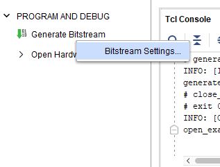
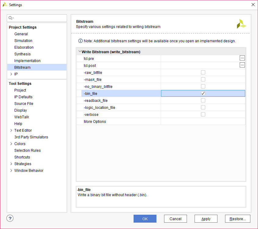
Step 1: It is recommended to generate .bin bitstream file along with .bit bitstream file. Right Click on “Bitstream Settings”.
Step 2: Select “-bin_file*” option in the dialog window and Click “OK”.
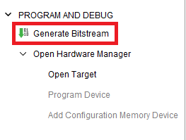
Step 3: Finally click “Generate Bitstream”.
Configuring HSFPX002 Module
Configuring HSFPX002 Module Using JTAG
To configure HSFPX002 Module using JTAG, a carrier board is required such as Numato Lab’s HSFPX00X board which features a JTAG connector which facilitates easy reprogramming of SRAM and on-board SPI flash through JTAG programmer like “XILINX Platform Cable USB”. Programming HSFPX002 using JTAG requires “XILINX Vivado Hardware Manager” software which is bundled with XILINX Vivado Design Suite. To program the SPI flash we need a “.mcs/.bin” file that needs to be generated from the “.bit” file. Steps for generating “.mcs/.bin” file are as below. Programming FPGA SRAM does not require a “.mcs/.bin” file to be generated.
Programming FPGA using Vivado
Step 1: By using JTAG cable, connect Xilinx platform cable USB to HSFPX002 and power it up.
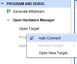
Step 2: Open Vivado project and open the target by clicking on the “Open Target” in “Open Hardware Manager” in the “Program and Debug” section of the Flow Navigator window. Select “Auto Connect”.
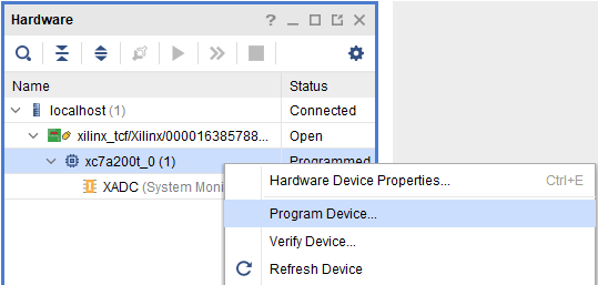
Step 3: If the device is detected successfully, to program the device, right click on the target device “xc7a200t_0” and select “Program Device” as shown below.
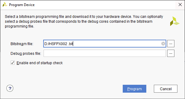
Step 4: In the dialog window which opens up, Vivado automatically chooses correct bitstream file if the design was synthesized, implemented and if the bitstream was generated successfully. If needed, browse to the bitstream which needs to be programmed to FPGA. Finally, click “Program”.
Generating Memory Configuration File for HSFPX002 using Vivado
The screenshots shown in the following steps are captured from the Vivado Design Suite 2018.2.
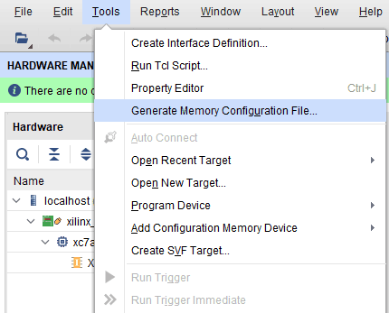
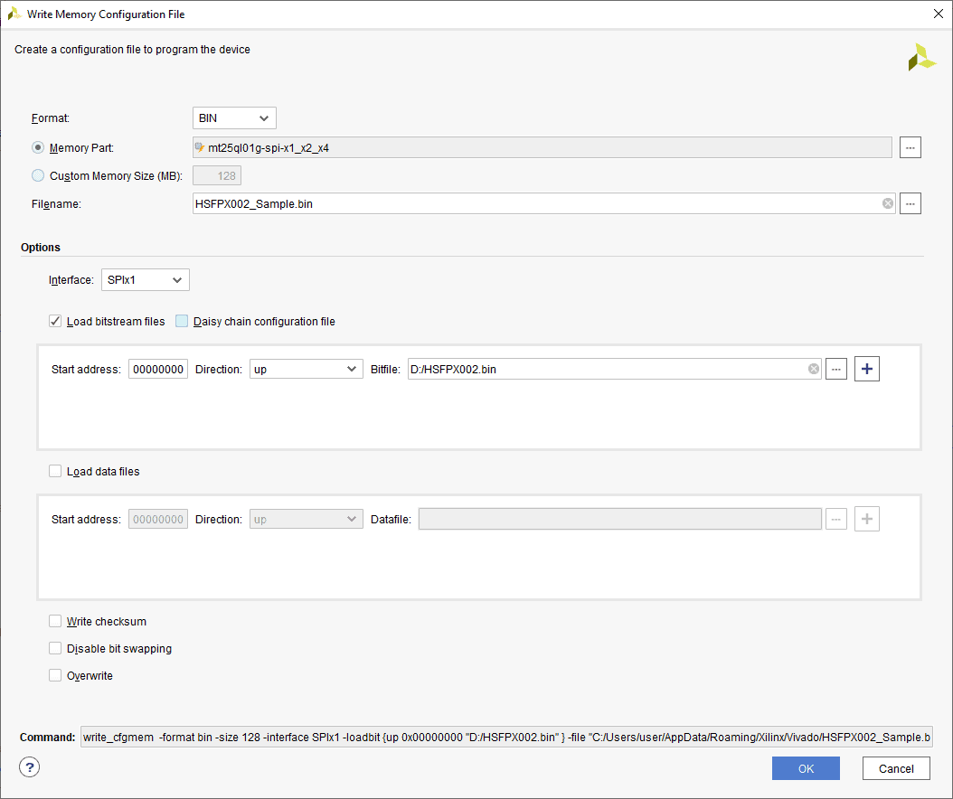
Step 1: Open Xilinx Vivado Hardware Manager. Connect the board, click “Generate Memory Configuration File….” from “Tools” menu. “Write Memory Configuration File” pop up window will open.
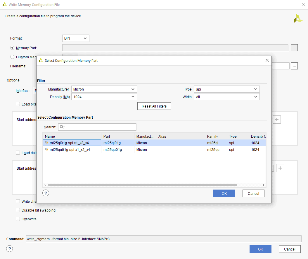
Step 2: Select the ‘Format’ and Configuration Memory Part as shown below. Choose the format as MCS/BIN/HEX depending on your requirement. Now, click “OK”.
Step 3: Browse to the path where you wish to save the Configuration File and type the file name as “sample.bin” (or any name as per your wish/requirement) to save the memory configuration file (the format of the file may change depending on your “Format”). Select the “Load bitstream files” under the ”Options” tab and browse to the “.bit” file we already generated then click “OK” to generate memory configuration file.
Programming QSPI Flash using Vivado
A .bin or .mcs file is required for programming HSFPX002’s onboard QSPI flash.
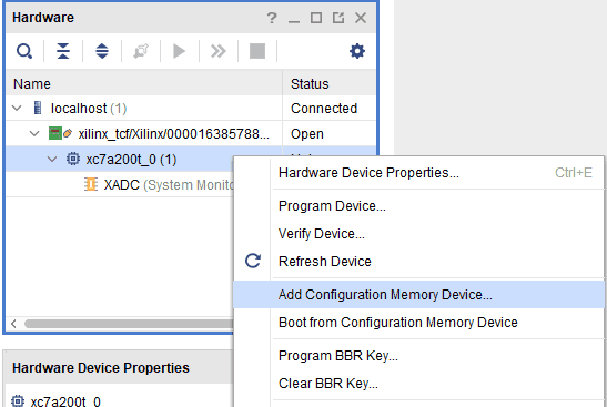
Step 1: Open the Vivado project and open the target by clicking on the “Open Target” in “Open Hardware Manager” in the “Program and Debug” section of the Flow Navigator window. Select “Auto Connect”.
Step 2: If the device is detected successfully, it will be displayed as shown in the image below. To add Configuration Memory Device, right-click on the target device “xc7a200t_0” and select “Add Configuration Memory Device” as shown below.
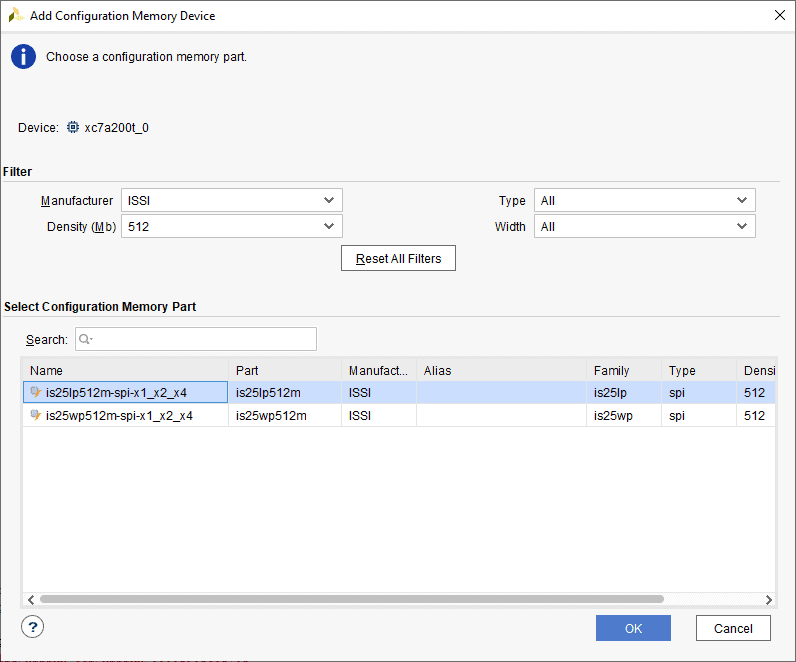
Step 3: Select the memory device “is25lp512m-spi-x1_x2_x4”, then click OK.
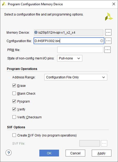
Step 4: Browse to the working .bin file or the .mcs file (whichever is applicable) and click OK to program as shown below. If programming is successful, a confirmation message will be displayed.
Technical Specifications
| Parameter* | Value | Unit |
|---|---|---|
| Basic Specifications | ||
| GPIOs | 96 | |
| 2 x DDR3 SDRAM (MT41K512M16HA-125) | 512 | Mb |
| DDR3 SDRAM (MT41K1G8SN-125) | 1 | Gb |
| On-board Oscillator Frequency (ASEM1-100.000Mhz-LC-T) | 100 | MHz |
| SPI Flash Memory (S25FL512SDSBHV210/IS25LP512M-RHLE) | 512 | Mb |
| LEDs | 1 (Bi-color LED) | |
| FPGA Specifications | ||
| Internal supply voltage relative to GND | -0.5 to 1.1 | V |
| Axuiliary supply voltage relative to GND | -0.5 to 2.0 | V |
| Output driver supply voltage relative to GND | -0.5 to 3.6 | V |
* All parameters considered nominal. Numato Systems Pvt Ltd reserves the right to modify products without notice.
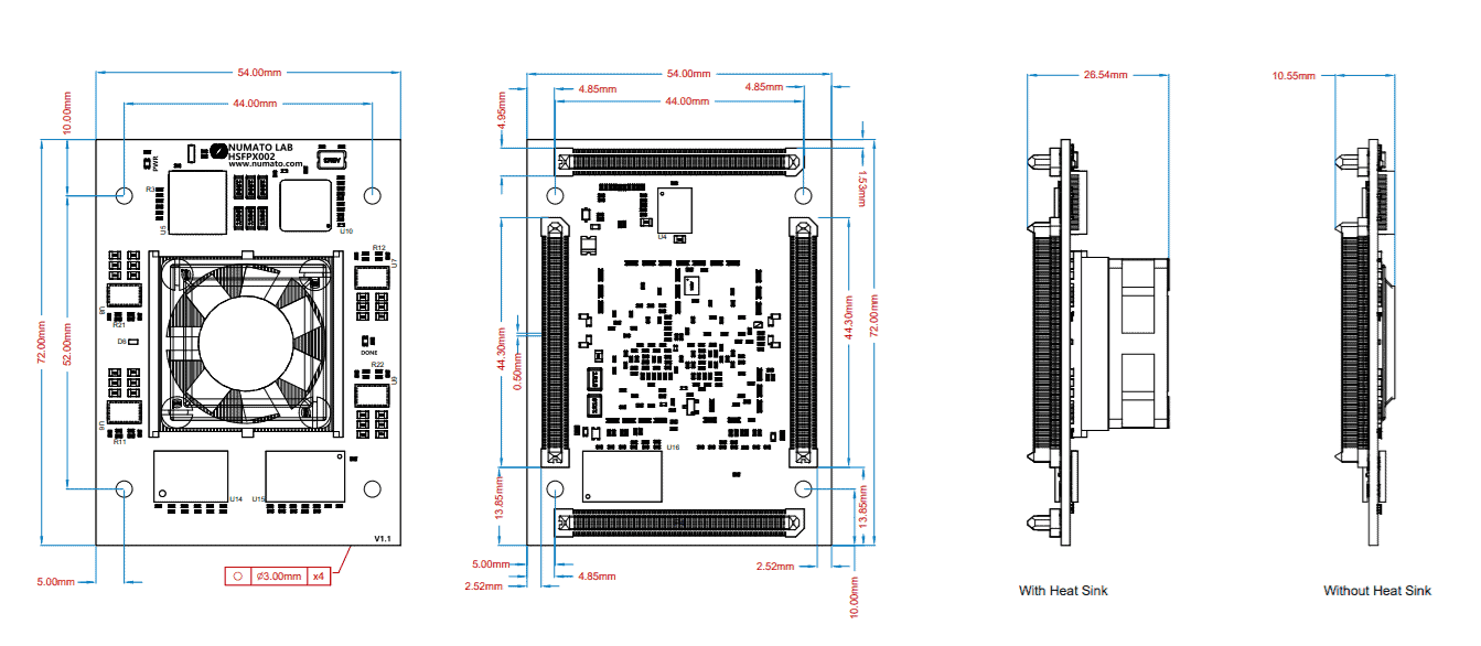
Mechanical Dimensions