

1.Introduction
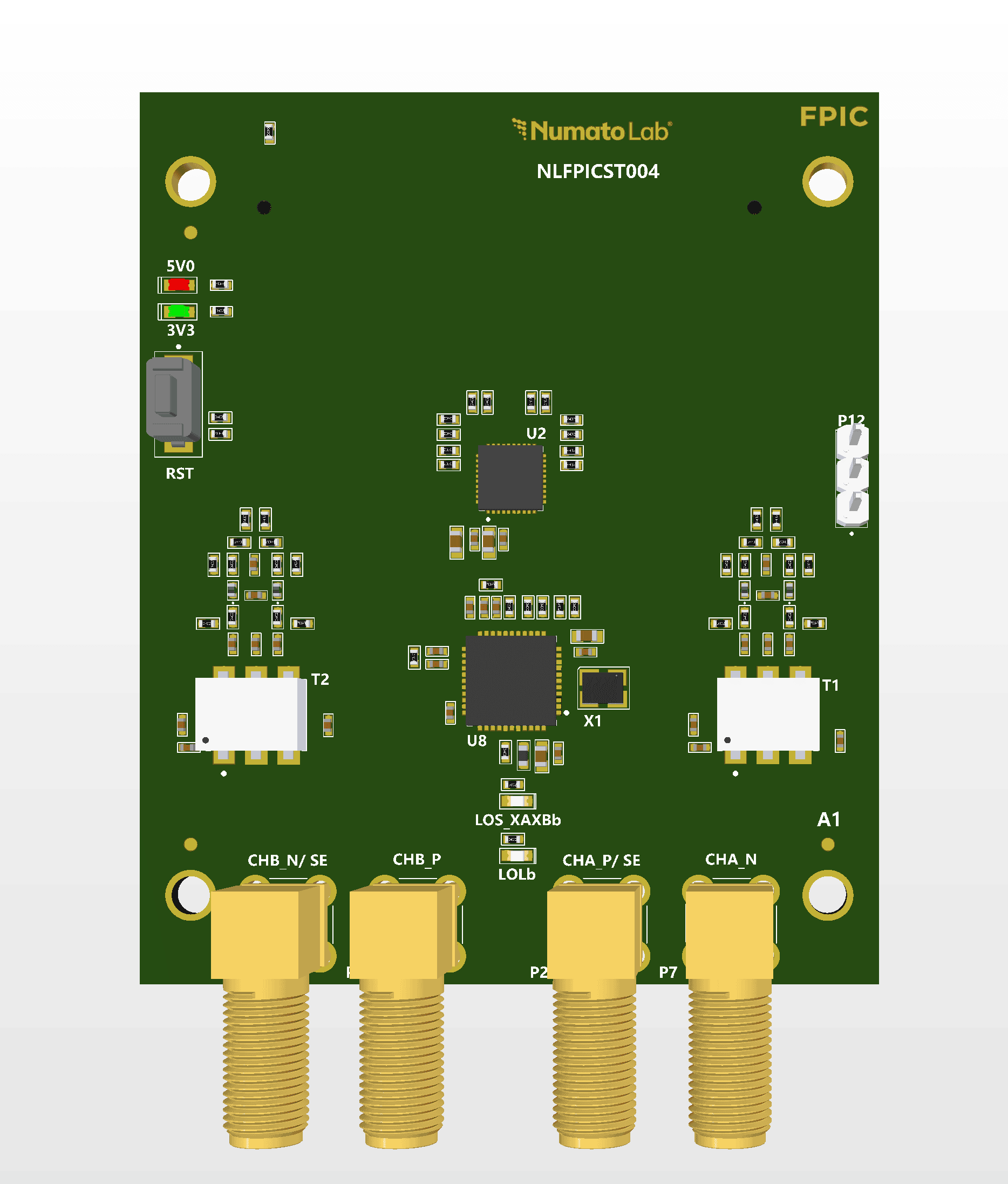
The FPIC ADC Module is a high-performance ADC expansion module designed for FPGA development boards that support the FPICST (FPGA Peripheral Interface Connector) standard. The module provides a flexible and modular solution for integrating analog-to-digital conversion capabilities into FPGA-based data acquisition and signal processing systems.
The module supports the ADC366x series and interfaces with the FPGA development board through the standardized FPICST connector, providing the necessary electrical connections for ADC data transfer, clocking, configuration, and control signals.
The module also incorporates an onboard SI5340A clock generator to generate the sampling clock and digital clock signals required by the ADC, ensuring the necessary clocking for reliable data acquisition and transfer. This standardized interface enables compatibility with supported FPGA platforms without requiring board-specific modifications to the ADC module.
 Was this helpful?

2.Applications
-
High-speed analog data acquisition.
-
Real-time digital signal processing.
-
Analog waveform monitoring and analysis.
-
FPGA-based test and measurement systems.
-
Communication signal acquisition and processing.
-
Industrial sensor monitoring.
-
Continuous analog data logging.
-
FPGA-based embedded data acquisition systems.
3.Features
-
ADC Support: Supports the ADC366x series.
-
FPIC ST Interface: Provides a standardized FPIC connector for interfacing with compatible FPGA boards.
-
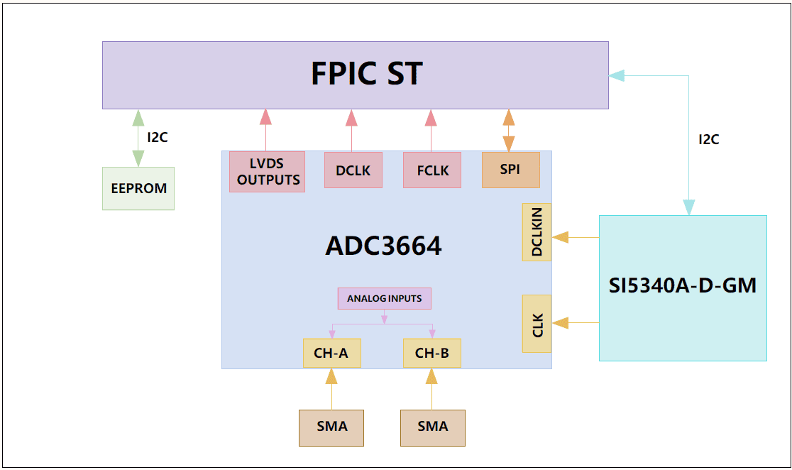
Dual Analog Input Channels: Supports two independent analog input channels (CH-A and CH-B).
-
SMA Connectors: Provides dedicated SMA connectors for analog signal inputs.
-
LVDS Data Interface: Supports LVDS outputs for ADC data transfer to the FPGA.
-
SPI Configuration: Enables ADC configuration and control through the SPI interface.
-
Clock Generation: Incorporates the SI5340A clock generator for generating the required ADC sampling and digital clock signals.
-
I2C Interface: Provides I2C communication between the FPGA and the clock generator.
-
EEPROM Support: Includes an onboard EEPROM for module identification and configuration information.
-
Modular Design: Enables integration with compatible FPGA platforms through the standardized FPIC interface.
4.Functional Block Diagram
5.Connection Diagram
6.Connection Details
| SL No. | Signal | FPIC Pin Location | Signal Detail |
|---|---|---|---|
| 1 | DCLK_P | IO0_P/CLK0_P | ADC Data Clock+ → FPGA |
| 2 | DCLK_N | IO0_N/CLK0_N | ADC Data Clock- → FPGA |
| 3 | FCLK_P | IO1_P/CLK1_P | ADC Frame Clock+ → FPGA |
| 4 | FCLK_N | IO1_N/CLK1_N | ADC Frame Clock- → FPGA |
| 5 | DA0_P | IO2_P | ADC Channel A Data Lane 0+ |
| 6 | DA0_N | IO2_N | ADC Channel A Data Lane 0- |
| 7 | DA1_P | IO3_P | ADC Channel A Data Lane 1+ |
| 8 | DA1_N | IO3_N | ADC Channel A Data Lane 1- |
| 9 | DB0_P | IO4_P | ADC Channel B Data Lane 0+ |
| 10 | DB0_N | IO4_N | ADC Channel B Data Lane 0- |
| 11 | DB1_P | IO5_P | ADC Channel B Data Lane 1+ |
| 12 | DB1_N | IO5_N | ADC Channel B Data Lane 1- |
| 13 | SDIO | IO6_P | ADC SPI Data I/O |
| 14 | SEN | IO6_N | ADC SPI Chip Select (CS) |
| 15 | SCLK | IO7_P | ADC SPI Clock |
| 16 | SDI | IO7_N | ADC SPI Data Input |
| 17 | PDN/SYNC | IO8_P | ADC Power-Down / Synchronization Control |
| 18 | RESET | IO8_N | ADC Reset Control |
| 19 | CLOCK_SCLK | IO9_P | Clock Generator I²C SCL |
| 20 | CLOCK_SDA | IO9_N | Clock Generator I²C SDA |
| 21 | GA0 | GA0 | EEPROM Address Select GA0 |
| 22 | GA1 | GA1 | EEPROM Address Select GA1 |
| 23 | SCL | SCL | EEPROM I²C SCL |
| 24 | SDA | SDA | EEPROM I²C SDA |
7.Technical Specification
| SL No. | Parameter | Value | Unit |
|---|---|---|---|
| 1 | Module Name | FPICST04-High Speed & Low Speed ADC Module | |
| 2 | ADC Support | ADC3664 / ADC3661 | |
| 3 | ADC Channels | 2 (CH-A, CH-B) | Channels |
| 4 | Analog Input Connector | SMA | |
| 5 | Connector Standard | FPIC-ST | |
| 6 | ADC Data Interface | LVDS | |
| 7 | ADC Configuration Interface | ||
| 8 | Clock Generator | SI5340A | |
| 9 | Clock Generator Interface | I²C | |
| 10 | EEPROM | 24AA025E64T-I/SN | |
| 11 | EEPROM Capacity | 2 | Kbit |
8.Mechanical Dimensions
9.FPIC ADC Variant Specifications
| SL No. | Parameter | ADC3664 | ADC3663 | ADC3662 | ADC3661 | Unit |
|---|---|---|---|---|---|---|
| 1 | ADC Resolution | 14 | 16 | 16 | 16 | Bits |
| 2 | Maximum Sampling Rate | 125 | 65 | 25 | 10 | MSPS |
| 3 | Number of Channels | 2 | 2 | 2 | 2 | Channels |
| 4 | Digital Output Interface | Serial LVDS | Serial LVDS | Serial LVDS | Serial LVDS |
10.SI5340A Default configuration according to ADC variant
| SL No. | ADC Variant | SI5340A - OUT0 Frequency(Sampling clock) | SI5340A - OUT1 Frequency(Data Clock) | Unit |
|---|---|---|---|---|
| 1 | ADC3664 | 125 | 437.5 | MHz |
| 2 | ADC3663 | 65 | 227.5 | MHz |
| 3 | ADC3662 | 25 | 87.5 | MHz |
| 4 | ADC3661 | 10 | 35 | MHz |