Introduction
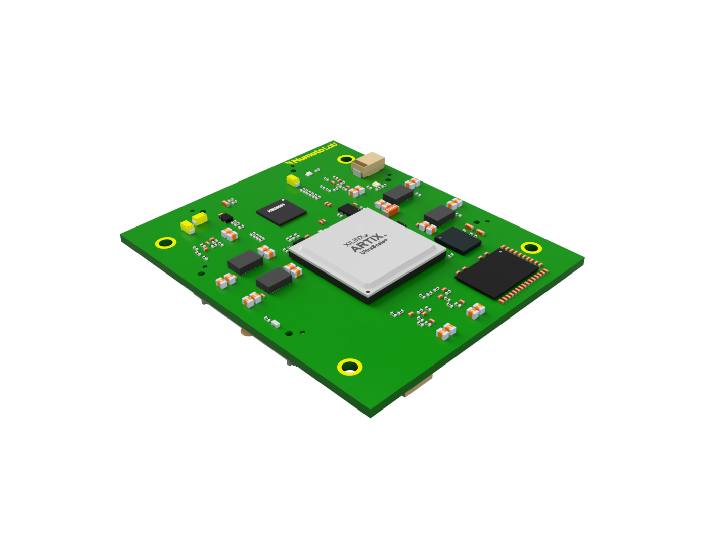 Introducing the EagleCore AU-Plus Development Kit – NL001 – a groundbreaking System-on-Module designed to deliver unparalleled performance and versatility.
At its heart lies the formidable Artix Ultrascale+ FPGA, providing a robust platform for advanced programmability. This compact module is meticulously crafted, featuring essential components such as DDR, Ethernet, and QSPI Flash. The inclusion of DDR ensures efficient data processing, while Ethernet facilitates high-speed networking, and QSPI Flash ensures reliable and swift storage solutions.
The Artix Ultrascale+ FPGA, renowned for its power and flexibility, positions the EagleCore Development Kit as an ideal solution for a wide array of embedded systems and digital design applications. Elevate your projects with the advanced capabilities of the EagleCore AU-Plus Development Kit.
Board Features
- Device: Artix Ultrascale+ (XCAU25P-1FFVB676I).
- SDRAM – DDR4.
- Flash Memory: 1 Gb SPI flash memory.
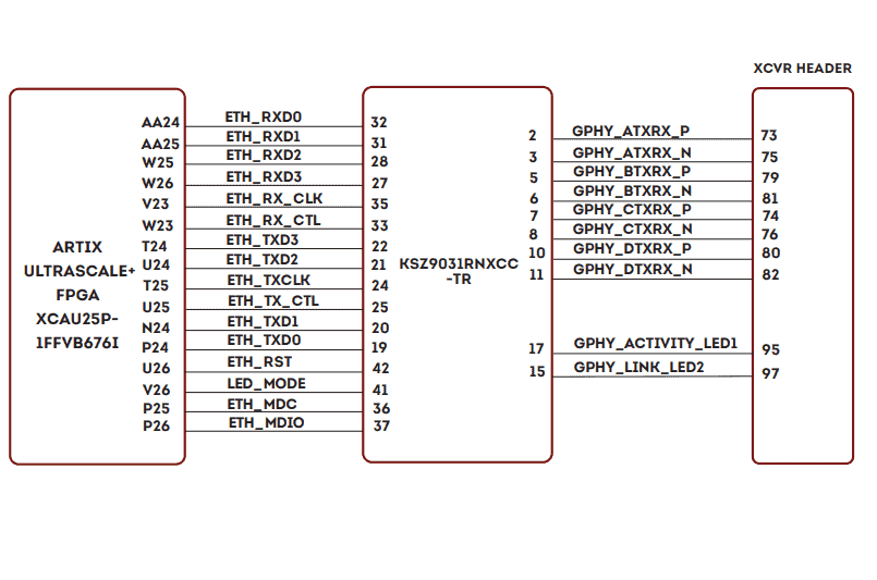
- 1 x Gigabit Ethernet PHY.
- 100MHz CMOS oscillator (Fabric clock).
- 100MHz DDR4 Reference Clock.
- 125MHz MGT Reference Clock.
- Trusted Platform Module.
- OTG PHY.
- EEPROM.
- 4x Razor Beam LSHM Series Samtec Connectors.
- Programming & Debugging: JTAG programming.
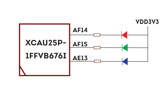
- 1 RGB LED for custom use.
- RTC (BQ32000DR).
- 84 differential GPIOs and 18 differential GTH pins for user-defined purposes.
Application
- Artificial Intelligence (AI)
- Industrial Automation
- Embedded Vision
- High-Performance Computing (HPC)
- Aerospace and Defense
- Communication and Networking
How to use EagleCore AU-Plus Development Kit
The following sections describe in detail how to use this module.
Hardware Accessories Required
- 5V DC Power Supply.
- EagleCore Carrier Board.
- Xilinx Platform Cable USB II JTAG debugger.
- USB Type C cable.
Connection Diagram
Please note that the diagram provided is intended solely as a reference. 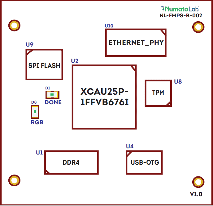
RGB LED
EagleCore AU-Plus Development Kit features an RGB LED which can be used for customizing or debugging purposes. The LED is wired in the active-low configuration.
Ethernet
The KSZ9031RNX is a completely integrated triple-speed (10BASE-T/100BASE-TX/1000BASE-T) Ethernet physical layer transceiver for transmission and reception of data. It provides the Reduced Gigabit Media Independent Interface (RGMII) for direct connection to RGMII MACs in Gigabit Ethernet processors and switches for data transfer at 10/100/1000 Mbps.
DDR4
EagleCore AU-Plus Development Kit uses DDR4(MT40A512M16LY-075:E) which is a high-speed dynamic random-access memory internally configured as an eight-bank DRAM. The DDR4 SDRAM uses an 8n-prefetch architecture to achieve high-speed operation. The 8n-prefetch architecture is combined with an interface designed to transfer two data words per clock cycle at the I/O pins. DDR4 is connected to the bank 64 of Artix Ultrascale+ FPGA.
| Function | FPGA pin |
|---|---|
| DDR4-DQ0 | AF24 |
| DDR4-DQ1 | AB25 |
| DDR4-DQ2 | AB26 |
| DDR4-DQ3 | AC24 |
| DDR4-DQ4 | AF25 |
| DDR4-DQ5 | AB24 |
| DDR4-DQ6 | AD24 |
| DDR4-DQ7 | AD25 |
| DDR4-DQ8 | AB21 |
| DDR4-DQ9 | AE21 |
| DDR4-DQ10 | AE23 |
| DDR4-DQ11 | AD23 |
| DDR4-DQ12 | AC23 |
| DDR4-DQ13 | AD21 |
| DDR4-DQ14 | AC22 |
| DDR4-DQ15 | AC21 |
| DDR4-A0 | AD18 |
| DDR4-A1 | AE17 |
| DDR4-A2 | AB17 |
| DDR4-A3 | AE18 |
| DDR4-A4 | AD19 |
| DDR4-A5 | AF17 |
| DDR4-A6 | Y17 |
| DDR4-A7 | AE16 |
| DDR4-A8 | AA17 |
| DDR4-A9 | AC17 |
| DDR4-A10_AP | AC19 |
| DDR4-A11 | AC16 |
| DDR4-A122_BC_n | AF20 |
| DDR4-A13 | AD16 |
| DDR4-A14_WE_n | AA19 |
| DDR4-A15_CAS_n | AF19 |
| DDR4-A16_RAS_n | AA18 |
| DDR4_DM0 | AE25 |
| DDR4_DM1 | AE22 |
| DDR4-RESET_n | AE26 |
| DDR4_DQS0_P | AC26 |
| DDR4_DQS0_N | AD26 |
| DDR4_DQS1_P | AA22 |
| DDR4_DQS1_N | AB22 |
| DDR4-CS_n | AF22 |
| DDR4-BA0 | AC18 |
| DDR4-BA1 | AF18 |
| DDR4-CK_P | Y20 |
| DDR4-CK_N | Y21 |
| DDR4-BG0 | AB19 |
| DDR4-CKE | AA20 |
| DDR4-ODT | AB20 |
| DDR4-ACT_n | Y18 |
SPI_FLASH
The SOM has 1 Gb of Quad bit SPI flash memory. It is a serial NOR flash which operates at the voltage of 1.8 V. It serves as the default primary boot device.
| QSPI Pins | FPGA Pins |
|---|---|
| SPI_DQ0 | AD11 |
| SPI_DQ1 | AC12 |
| SPI_DQ2 | AC11 |
| SPI_DQ3 | AE11 |
| SPI_CS_N | AA12 |
| SPI_RST# | R26 |
| SPI_SCK | Y11 |
Trusted Platform Module(TPM)
The Trusted Platform Module(TPM) is an integrated security module for hardware authentication. The security module is used primarily for cryptographic key generation, key storage and key management as well as generation and secure storage for digital certificates.
| Signal Name | FPGA PIN |
|---|---|
| TPM_CLK | G10 |
| TPM_RST | H9 |
| TPM_CS | G9 |
| TPM_MOSI | H11 |
| TPM_MISO | G11 |
Clock and Reset
| Clock and reset Pins | FPGA Pins |
|---|---|
| REF_CLK_P | V24 |
| REF_CLK_N | W24 |
| DEVRST_n | AF13 |
OTG PHY
| Signal Name | FPGA PIN |
|---|---|
| USB_STP | Y26 |
| USB_OTG_RST | R25 |
| USB_NXT | Y23 |
| USB_DIR | Y25 |
| USB_D7 | W20 |
| USB_D6 | W19 |
| USB_D5 | T23 |
| USB_D4 | T22 |
| USB_D3 | V22 |
| USB_D2 | V21 |
| USB_D1 | U20 |
| USB_D0 | T20 |
| USB_CLK | Y22 |
EEPROM
| Signal Name | FPGA PIN |
|---|---|
| MAC_SCL | F10 |
| MAC_SDA | F9 |
GPIOs
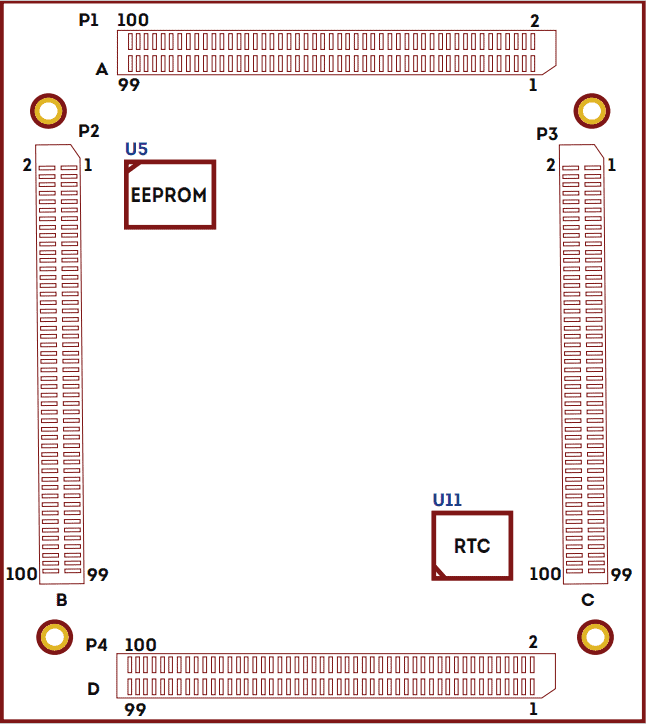
Header P3
| Pin No. on Connector | Pin Name | FPGA PIN | Pin No. on Connector | Pin Name | FPGA PIN |
|---|---|---|---|---|---|
| 1 | VIN | 2 | VIN | ||
| 3 | VIN | 4 | VIN | ||
| 5 | VIN | 6 | VIN | ||
| 7 | GND | 8 | GND | ||
| 9 | GND | 10 | GND | ||
| 11 | VDD1V8 | 12 | VDD1V8 | ||
| 13 | VDD1V8 | 14 | VDD1V8 | ||
| 15 | GND | 16 | GND | ||
| 17 | B87_IO0_CC_P | G12 | 18 | B87_IO2_P | E13 |
| 19 | B87_IO0_CC_N | F12 | 20 | B87_IO2_N | E12 |
| 21 | B87_IO1_P | A13 | 22 | B87_IO3_P | C12 |
| 23 | B87_IO1_N | A12 | 24 | B87_IO3_N | B12 |
| 25 | GND | 26 | GND | ||
| 27 | B87_IO4_P | H14 | 28 | B87_IO6_CC_P | J12 |
| 29 | B87_IO4_N | G14 | 30 | B87_IO6_CC_N | H12 |
| 31 | B87_IO5_P | J15 | 32 | B87_IO7_CC_P | J13 |
| 33 | B87_IO5_N | J14 | 34 | B87_IO7_CC_N | H13 |
| 35 | GND | 36 | GND | ||
| 37 | B87_IO8_P | C14 | 38 | B87_IO10_CC_P | F14 |
| 39 | B87_IO8_N | C13 | 40 | B87_IO10_CC_N | F13 |
| 41 | B87_IO9_P | B14 | 42 | B87_IO11_P | D14 |
| 43 | B87_IO9_N | A14 | 44 | B87_IO11_N | D13 |
| 45 | GND | 46 | GND | ||
| 47 | B86_IO1_P | D9 | 48 | B86_IO3_P | B10 |
| 49 | B86_IO1_N | C9 | 50 | B86_IO3_N | A10 |
| 51 | B86_IO2_P | B9 | 52 | B86_IO4_P | D11 |
| 53 | B86_IO2_N | A9 | 54 | B86_IO4_N | D10 |
| 55 | GND | 56 | GND | ||
| 57 | B86_IO5_P | E11 | 58 | B84_IO1_P | AD13 |
| 59 | B86_IO5_N | E10 | 60 | B84_IO1_N | AD14 |
| 61 | B86_IO6_P | C11 | 62 | B84_IO2_P | AD15 |
| 63 | B86_IO6_N | B11 | 64 | B84_IO2_N | AE15 |
| 65 | GND | 66 | GND | ||
| 67 | B84_IO3_P | AC13 | 68 | B84_IO5_P | Y15 |
| 69 | B84_IO3_N | AC14 | 70 | B84_IO5_N | AA15 |
| 71 | B84_IO4_P | W14 | 72 | B84_IO6_P | AA14 |
| 73 | B84_IO4_N | W15 | 74 | B84_IO6_N | AB14 |
| 75 | GND | 76 | GND | ||
| 77 | B84_IO7_P | Y13 | 78 | B84_IO9_P | AB15 |
| 79 | B84_IO7_N | AA13 | 80 | B84_IO9_N | AB16 |
| 81 | B84_IO8_P | W12 | 82 | B84_IO10_P | W16 |
| 83 | B84_IO8_N | W13 | 84 | B84_IO10_N | Y16 |
| 85 | GND | 86 | GND | ||
| 87 | USB_OTG_D_N | 88 | USB_ID | ||
| 89 | USB_OTG_D_P | 90 | USB_5V | ||
| 91 | TDI | 92 | TDO | ||
| 93 | TMS | 94 | TCK | ||
| 95 | NC | 96 | DEVRST_n | AF13 | |
| 97 | NC | 98 | NC | ||
| 99 | GND | 100 | GND |
Header P2
| Pin No. on Connector | Pin Name | FPGA PIN | Pin No. on Connector | Pin Name | FPGA PIN |
|---|---|---|---|---|---|
| 1 | VIN | 2 | VIN | ||
| 3 | VIN | 4 | VIN | ||
| 5 | VIN | 6 | VIN | ||
| 7 | GND | 8 | GND | ||
| 9 | GND | 10 | GND | ||
| 11 | VDD1V8 | 12 | VDD1V8 | ||
| 13 | VDD1V8 | 14 | VDD1V8 | ||
| 15 | GND | 16 | GND | ||
| 17 | B66_IO0_P | M19 | 18 | B66_IO2_P | M20 |
| 19 | B66_IO0_N | L19 | 20 | B66_IO2_N | M21 |
| 21 | B66_IO1_P | L18 | 22 | B66_IO3_P | L20 |
| 23 | B66_IO1_N | K18 | 24 | B66_IO3_N | K20 |
| 25 | GND | 26 | GND | ||
| 27 | B66_IO4_P | J19 | 28 | B66_IO6_P | H21 |
| 29 | B66_IO4_N | J20 | 30 | B66_IO6_N | H22 |
| 31 | B66_IO5_P | K21 | 32 | B66_CC_IO7_P | J23 |
| 33 | B66_IO5_N | J21 | 34 | B66_CC_IO7_N | J24 |
| 35 | GND | 36 | GND | ||
| 37 | B66_CC_IO8_P | K22 | 38 | B66_CC_IO10_P | H23 |
| 39 | B66_CC_IO8_N | K23 | 40 | B66_CC_IO10_N | H24 |
| 41 | B66_IO9_P | L22 | 42 | B66_IO11_P | F23 |
| 43 | B66_IO9_N | L23 | 44 | B66_IO11_P | E23 |
| 45 | GND | 46 | GND | ||
| 47 | B66_IO12_P | L24 | 48 | B66_IO14_P | D23 |
| 49 | B66_IO12_N | L25 | 50 | B66_IO14_N | C24 |
| 51 | B66_IO13_P | F24 | 52 | B66_IO15_P | D24 |
| 53 | B66_IO13_N | F25 | 54 | B66_IO15_N | D25 |
| 55 | GND | 56 | GND | ||
| 57 | B66_CC_IO16_P | G24 | 58 | B66_IO18_P | B25 |
| 59 | B66_CC_IO16_N | G25 | 60 | B66_IO18_N | B26 |
| 61 | B66_IO17_P | D26 | 62 | B66_IO19_P | E25 |
| 63 | B66_IO17_P | C26 | 64 | B66_IO19_N | E26 |
| 65 | GND | 66 | GND | ||
| 67 | B66_IO20_P | H26 | 68 | B66_IO22_P | K25 |
| 69 | B66_IO20_N | G26 | 70 | B66_IO22_N | K26 |
| 71 | B66_IO21_P | J25 | 72 | B66_IO23_P | M25 |
| 73 | B66_IO21_N | J26 | 74 | B66_IO23_N | M26 |
| 75 | GND | 76 | GND | ||
| 77 | B65_IO0_P | N19 | 78 | B65_IO2_P | N21 |
| 79 | B65_IO0_N | P19 | 80 | B65_IO2_N | N22 |
| 81 | B65_IO1_P | P20 | 82 | B65_IO3_P | N23 |
| 83 | B65_IO1_N | P21 | 84 | B65_IO3_P | P23 |
| 85 | GND | 86 | GND | ||
| 87 | B65_IO4_P | R20 | 88 | B65_IO6_P | U21 |
| 89 | B65_IO4_N | R21 | 90 | B65_IO6_N | U22 |
| 91 | B65_IO5_P | R22 | 92 | B65_IO7_P | U19 |
| 93 | B65_IO5_N | R23 | 94 | B65_IO7_N | V19 |
| 95 | NC | 96 | NC | ||
| 97 | NC | 98 | NC | ||
| 99 | GND | 100 | GND |
Header P1
| Pin No. on Connector | Pin Name | FPGA PIN | Pin No. on Connector | Pin Name | FPGA PIN |
|---|---|---|---|---|---|
| 1 | VDD1V2 | 2 | VDD1V8 | ||
| 3 | VDD1V2 | 4 | VDD1V8 | ||
| 5 | GND | 6 | GND | ||
| 7 | MGTREFCLK0_224_P | AB7 | 8 | DP0_CLK0_P | |
| 9 | MGTREFCLK0_224_N | AB6 | 10 | DP0_CLK0_N | |
| 11 | GND | 12 | GND | ||
| 13 | MGTHRX0_224_P | AF2 | 14 | MGTHTX0_224_P | AF7 |
| 15 | MGTHRX0_224_N | AF1 | 16 | MGTHTX0_224_N | AF6 |
| 17 | GND | 18 | GND | ||
| 19 | MGTHRX1_224_P | AE4 | 20 | MGTHTX1_224_P | AE9 |
| 21 | MGTHRX1_224_N | AE3 | 22 | MGTHTX1_224_N | AE8 |
| 23 | GND | 24 | GND | ||
| 25 | MGTHRX2_224_P | AD2 | 26 | MGTHTX2_224_P | AD7 |
| 27 | MGTHRX2_224_N | AD1 | 28 | MGTHTX2_224_N | AD6 |
| 29 | GND | 30 | GND | ||
| 31 | MGTHRX3_224_P | AB2 | 32 | MGTHTX3_224_P | AC5 |
| 33 | MGTHRX3_224_N | AB1 | 34 | MGTHTX3_224_N | AC4 |
| 35 | GND | 36 | GND | ||
| 37 | MGTREFCLK1_225_P | T7 | 38 | NC | |
| 39 | MGTREFCLK1_225_N | T6 | 40 | NC | |
| 41 | GND | 42 | GND | ||
| 43 | MGTHRX0_225_P | Y2 | 44 | MGTHTX0_225_P | AA5 |
| 45 | MGTHRX0_225_N | Y1 | 46 | MGTHTX0_225_N | AA4 |
| 47 | GND | 48 | GND | ||
| 49 | MGTHRX1_225_P | V2 | 50 | MGTHTX1_225_P | W5 |
| 51 | MGTHRX1_225_N | V1 | 52 | MGTHTX1_225_N | W4 |
| 53 | GND | 54 | GND | ||
| 55 | MGTHRX2_225_P | T2 | 56 | MGTHTX2_225_P | U5 |
| 57 | MGTHRX2_225_N | T1 | 58 | MGTHTX2_225_N | U4 |
| 59 | GND | 60 | GND | ||
| 61 | MGTHRX3_225_P | P2 | 62 | MGTHTX3_225_P | R5 |
| 63 | MGTHRX3_225_N | P1 | 64 | MGTHTX3_225_N | R4 |
| 65 | GND | 66 | GND | ||
| 67 | NC | 68 | NC | ||
| 69 | NC | 70 | NC | ||
| 71 | GND | 72 | GND | ||
| 73 | GPHY_ATXRX_P | 74 | GPHY_CTXRX_P | ||
| 75 | GPHY_ATXRX_N | 76 | GPHY_CTXRX_N | ||
| 77 | GND | 78 | GND | ||
| 79 | GPHY_BTXRX_P | 80 | GPHY_DTXRX_P | ||
| 81 | GPHY_BTXRX_N | 82 | GPHY_DTXRX_N | ||
| 83 | GND | 84 | GND | ||
| 85 | NC | 86 | NC | ||
| 87 | CCC | 88 | NC | ||
| 89 | GND | 90 | GND | ||
| 91 | NC | 92 | NC | ||
| 93 | NC | 94 | NC | ||
| 95 | GPHY_ACTIVITY_LED1 | 96 | NC | ||
| 97 | GPHY_LINK_LED2 | 98 | NC | ||
| 99 | GND | 100 | GND |
Header P4
| Pin No. on Connector | Pin Name | FPGA PIN | Pin No. on Connector | Pin Name | FPGA PIN |
|---|---|---|---|---|---|
| 1 | VIN | 2 | VIN | ||
| 3 | VIN | 4 | VIN | ||
| 5 | VIN | 6 | VIN | ||
| 7 | GND | 8 | GND | ||
| 9 | GND | 10 | GND | ||
| 11 | VDD1V8 | 12 | VDD1V8 | ||
| 13 | VDD1V8 | 14 | VDD1V8 | ||
| 15 | GND | 16 | GND | ||
| 17 | B67_IO0_P | B15 | 18 | B67_IO2_P | E15 |
| 19 | B67_IO0_N | A15 | 20 | B67_IO2_N | D15 |
| 21 | B67_CC_IO1_P | E18 | 22 | B67_IO3_P | G15 |
| 23 | B67_CC_IO1_N | D18 | 24 | B67_IO3_N | F15 |
| 25 | GND | 26 | GND | ||
| 27 | B67_IO4_P | E16 | 28 | B67_IO6_P | H16 |
| 29 | B67_IO4_N | E17 | 30 | B67_IO6_N | G16 |
| 31 | B67_IO5_P | H17 | 32 | B67_IO7_P | D16 |
| 33 | B67_IO5_N | G17 | 34 | B67_IO7_N | C16 |
| 35 | GND | 36 | GND | ||
| 37 | B67_IO8_P | H18 | 38 | B67_CC_IO10_P | C18 |
| 39 | B67_IO8_N | H19 | 40 | B67_CC_IO10_ N | C19 |
| 41 | B67_IO9_P | G20 | 42 | B67_IO11_P | F18 |
| 43 | B67_IO9_N | G21 | 44 | B67_IO11_N | F19 |
| 45 | GND | 46 | GND | ||
| 47 | B67_IO12_P | C17 | 48 | B67_IO14_P | F20 |
| 49 | B67_IO12_N | B17 | 50 | B67_IO14_N | E20 |
| 51 | B67_IO13_P | A17 | 52 | B67_CC_IO15_P | D19 |
| 53 | B67_IO13_N | A18 | 54 | B67_CC_IO15_N | D20 |
| 55 | GND | 56 | GND | ||
| 57 | B67_CC_IO16_P | B19 | 58 | B67_IO18_P | E21 |
| 59 | B67_CC_IO16_N | B20 | 60 | B67_IO18_N | D21 |
| 61 | B67_IO17_P | A19 | 62 | B67_IO19_P | C22 |
| 63 | B67_IO17_N | A20 | 64 | B67_IO19_N | B22 |
| 65 | GND | 66 | GND | ||
| 67 | B67_IO20_P | C21 | 68 | B67_IO22_P | A24 |
| 69 | B67_IO20_N | B21 | 70 | B67_IO22_N | A25 |
| 71 | B67_IO21_P | C23 | 72 | B67_IO23_P | A22 |
| 73 | B67_IO21_N | B24 | 74 | B67_IO23_N | A23 |
| 75 | GND | 76 | GND | ||
| 77 | NC | 78 | NC | ||
| 79 | NC | 80 | NC | ||
| 81 | NC | 82 | NC | ||
| 83 | NC | 84 | NC | ||
| 85 | GND | 86 | GND | ||
| 87 | NC | 88 | NC | ||
| 89 | NC | 90 | NC | ||
| 91 | NC | 92 | NC | ||
| 93 | NC | 94 | NC | ||
| 95 | NC | 96 | NC | ||
| 97 | NC | 98 | NC | ||
| 99 | GND | 100 | GND |
Generating Bitstream for EagleCore AU-Plus Development Kit
The bitstream can be generated for EagleCore AU-Plus Development Kit in Vivado by following the steps below:
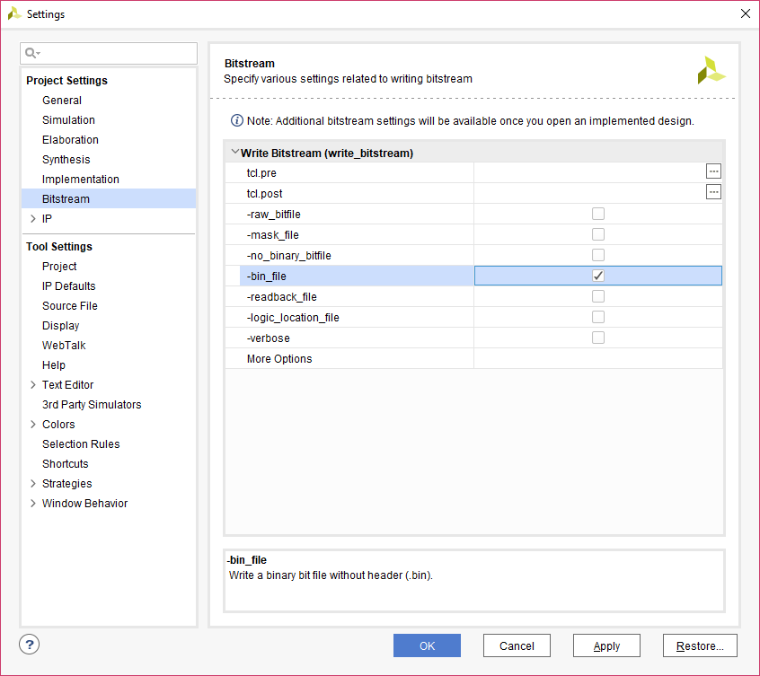
Step 1: It is recommended to generate a .bin bitstream file along with .bit bitstream file. Click “Bitstream Settings”.
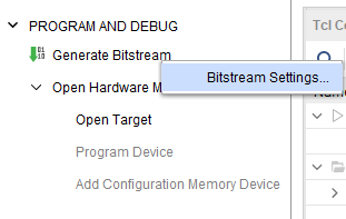
Step 2: In the window that pops up, select the “-bin_file*” option and click OK.
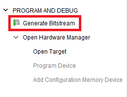
Step 3: Finally click “Generate Bitstream”.
Programming FPGA using JTAG
EagleCore AU-Plus Development Kit Carrier features an onboard JTAG connector that facilitates easy reprogramming of SRAM and onboard SPI flash through JTAG programmer like “Xilinx Platform cable USB”. The following steps illustrate how to program FPGA on Development Kit using JTAG.
Step1: By using JTAG cable, connect Xilinx platform cable USB to EagleCore AU-Plus Development Kit Carrier and power it up.
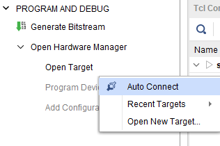
Step2: Open the Vivado project and open the target by clicking on the “Open Target” in “Open Hardware Manager” in the “Program and Debug” section of the Flow Navigator window. Select “Auto Connect”.
Step3: If the device is detected successfully, then select “Program Device” by right click on the target device “<add name>” as shown below.
<add image>
Step4: In the dialog window which opens up, Vivado automatically chooses the correct bitstream file if the design was synthesized, implemented and bitstream generated successfully. If needed, browse to the bitstream which needs to be programmed to FPGA. Finally, click “Program”.
<add image>.
Programming QSPI Flash using Vivado
A .bin or .mcs file is required for programming EagleCore AU-Plus Development Kit onboard QSPI flash.
Step 1: Open the Vivado project and open the target by clicking on the “Open Target” in “Open Hardware Manager” in the “Program and Debug” section of the Flow Navigator window. Select “Auto Connect”.
Step 2: If the device is detected successfully, then select “Add Configuration Memory Device” by right click on the target device “<name>” as shown below.
<add image>
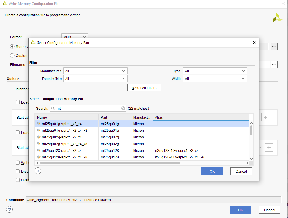
Step 3: Select the memory device “mt25qu01g-spi-x1_x2_x4” then click OK.
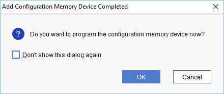
Step 4: After completion of Step 3 the following dialog box will open. Click OK.
Step 5: Browse to the working .bin file or the .mcs file (whichever applicable) and click OK to program as shown below. If programming is successful, a confirmation message will be displayed.
<add image>
Technical Specifications
| Parameter | Value | Unit |
|---|---|---|
| Basic Specifications | ||
| On-board oscillator frequency(ASDMPLV-100.000MZ-LR-T3) | 100 | MHz |
| Quad SPI Flash Memory(MT25QU01GBBB8E12-0AAT) | 1 | Gb |
| DDR4(MT40A512M16LY-075:E) | 8 | Gb |
| Power supply voltage (USB or External) | 5 | V |
| RGB LED | 1 | |
| FPGA Specifications | ||
| Internal supply voltage relative to GND | -0.5 to 1.1 | V |
| Auxiliary supply voltage relative to GND | -0.5 to 2.0 | V |
| Output drivers supply voltage for HD I/O banks | –0.500 to 3.400 | V |
| Output drivers supply voltage for HP I/O banks and configuration bank 0 | –0.500 to 2.000 | V |
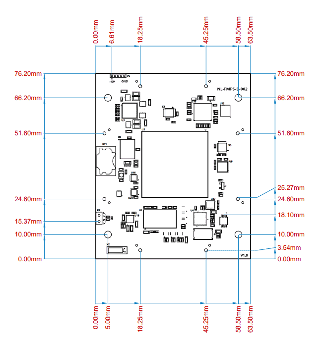
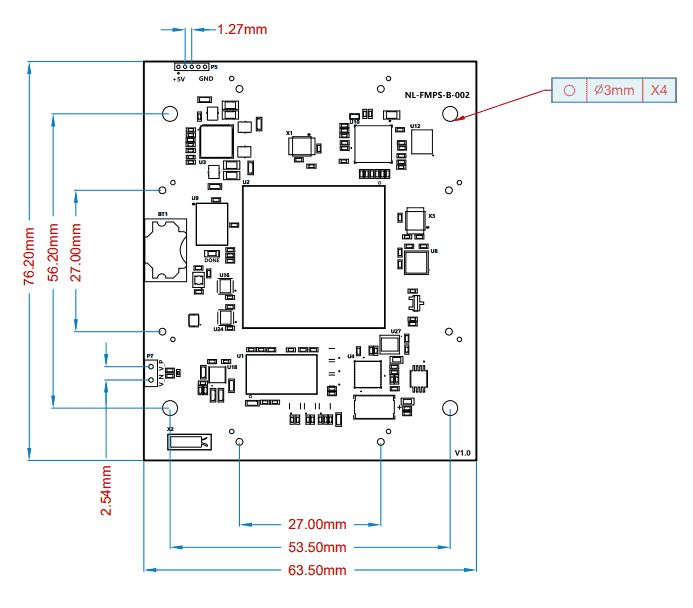
Mechanical Dimensions