
Introduction
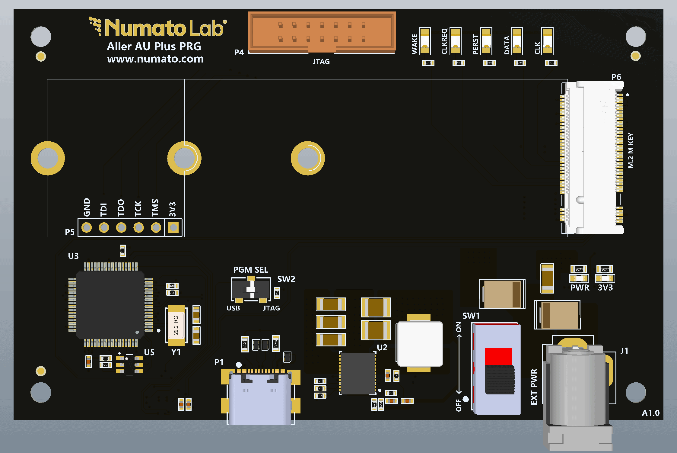
The Aller Programmer is designed to make programming and debugging of the Aller AU-Plus FPGA module straightforward and reliable. It integrates an onboard USB-JTAG interface and a standard JTAG header, both of which are routed through a multiplexer to the M.2 connector. The M.2 female connector on the programmer allows for a direct and secure connection to the Aller AU-Plus module, making it a compact and feature-rich programming platform.
Board Features
- JTAG header
- FTDI (FT2232H)
- USB type C
- M.2 key M
Hardware Accessories Required
- Aller AU-Plus Module.
- 5V DC Power supply
- USB-C cable
- AMD Platform Cable USB II compatible JTAG programmer
Power
The carrier can be powered either by connecting a 5V adapter to the DC jack or by connecting the USB cable.
Clock
M.2 Clock on the programmer
| Clock pins | FPGA pins |
|---|---|
| M.2_CLK_P | AA17 |
| M.2_CLK_N | AA18 |
JTAG Headers
The board features two JTAG headers: one with 6 pins and another with 14 pins. You can connect to either of these and set the SW2 switch to JTAG to program the module in JTAG mode.
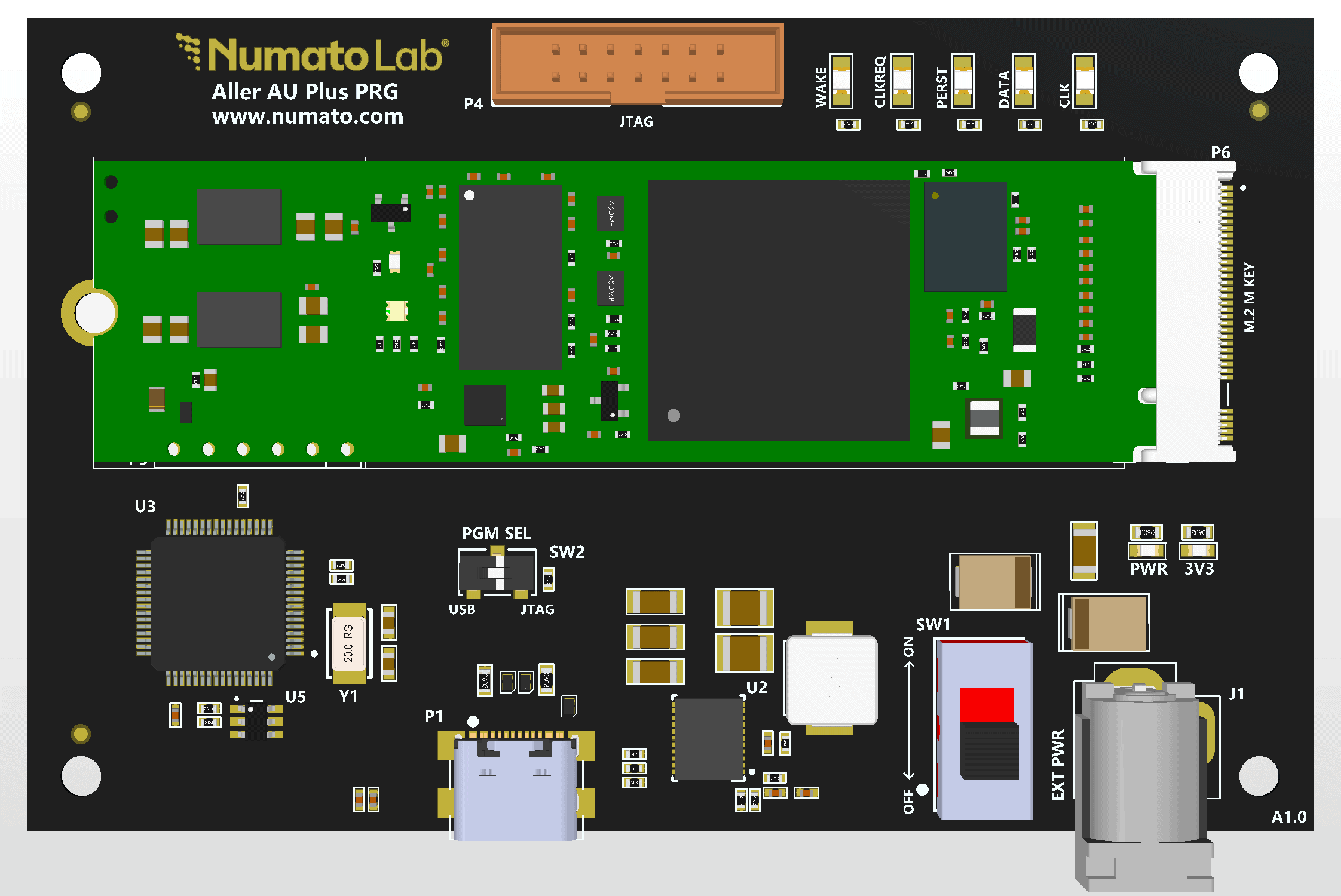
M.2 Edge Connector
The M.2 female connector on the programmer is used to connect the Aller AU-Plus Module to the carrier.
Programming Aller AU-Plus Module using Aller Programmer
Aller AU-Plus module can be programmed using two ways: Using JTAG header and USB-JTAG.
Connect the Aller AU-Plus Module to the M.2 female connector on the Aller Programmer before programming, as shown below.
Programming Aller AU-Plus Using JTAG
The onboard JTAG headers in the Aller programmer facilitates easy reprogramming of SRAM and SPI flash on the module through JTAG programmer like “AMD Platform cable USB”. Following steps illustrate how to program the FPGA on Aller AU-Plus module using JTAG header.
Step 1: Ensure that switch SW2 is set to JTAG mode.
Step 2: Connect the AMD Platform Cable USB to any one of the JTAG headers on the Programmer and power up the board.
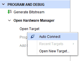
Step 3: Open Vivado project and open the target by clicking on the “Open Target” in “Open Hardware Manager” in the “Program and Debug” section of the Flow Navigator window. Select “Auto Connect”.
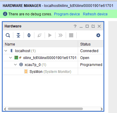
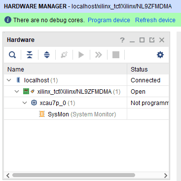
Step 4: If the device is detected successfully, then right click on the target device “xcau7p_0” and select “Program Device” as shown below.
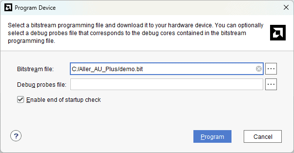
Step 5: In the dialog window which opens up, Vivado automatically chooses correct bitstream file if the design was synthesized, implemented and bitstream generated successfully. If needed, browse to the bitstream which needs to be programmed to FPGA. Finally, click “Program”.
As soon as “Program” is clicked, a orange colored DONE LED on Aller AU-Plus module should light up, indicating that programming process is going on. This LED will turn off when the configuration is complete.
Programming Aller AU-Plus Using USB-JTAG
Ensure that the D2XX drivers are installed prior to programming. The channel A of FTDI FT2232H chip on the Programmer is connected to the JTAG interface of the FPGA via the M.2 key socket. Through this connection, USB interface can be used as a JTAG programmer, eliminating the need for a dedicated JTAG cable or connector. Following steps illustrate how to program FPGA on Aller AU-Plus Module using USB-JTAG.
Step 1: Ensure that switch SW2 is set to USB mode.
Step 2: Connect the USB type C cable to the USB port on the Programmer and power up the board.
Step 3: Open Vivado project and open the target by clicking on the “Open Target” in “Open Hardware Manager” in the “Program and Debug” section of the Flow Navigator window. Select “Auto Connect”.
Step 4: If the device is detected successfully, then right click on the target device “xcau7p_0” and select “Program Device” as shown below.
Step 5: In the dialog window which opens up, Vivado automatically chooses correct bitstream file if the design was synthesized, implemented and bitstream generated successfully. If needed, browse to the bitstream which needs to be programmed to FPGA. Finally, click “Program”.
As soon as “Program” is clicked, an orange colored DONE LED on Aller AU-Plus module should light up, indicating that programming process is going on. This LED will turn off when the configuration is complete.
Programming QSPI Flash using Vivado
A ‘.bin’ or ‘.mcs’ file is required for programming Aller AU-Plus module’s onboard QSPI flash.
Step 1: Open Vivado Project. Click on “Open Target” in “Open Hardware Manager” in the “Program and Debug’ section of the Flow Navigator window. Select “Auto Connect”.
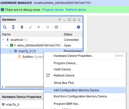
Step 2: If the device is detected successfully, then right-click on the target device “xcau7p_0” and select “Add Configuration Memory Device” as shown below.
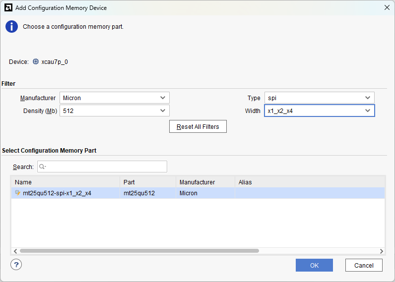
Step 3: Select the memory device “mt25qu512-spi-x1_x2_x4”, then click “OK”.
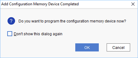
Step 4: After completion of Step 3 the following dialog box will open. Click “OK”.
Step 5: Browse to the working ‘.bin’ file or the ‘.mcs’ file (whichever is applicable) and click “Apply” and then “OK” to program as shown below. If programming is successful, a confirmation message will be displayed.