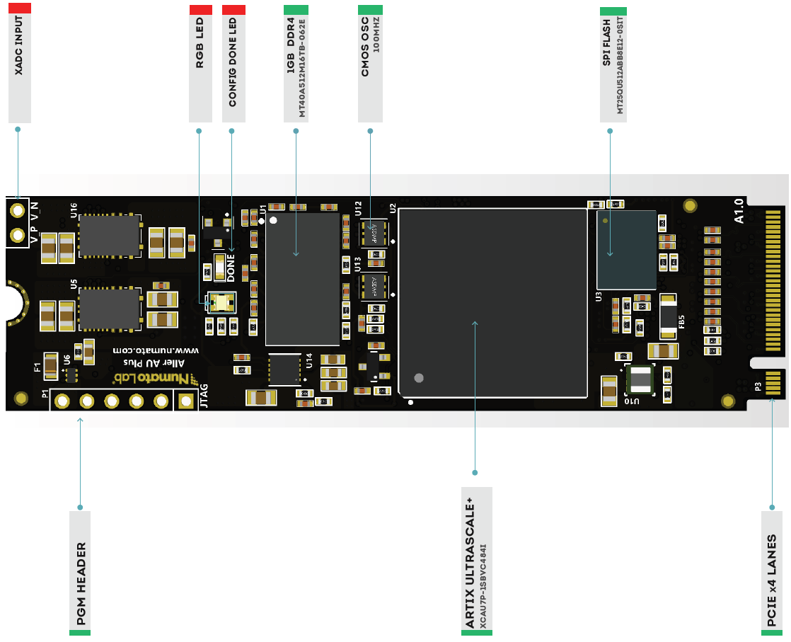
Onboard 512Mb QSPI flash memory for FPGA configuration
100 MHZ CMOS oscillator
1 x Trusted Platform Module (AT97SC3205)
M.2 Connector Interface, M-Key
Powered from M.2 connector
1 RGB LED for custom use
AMD Artix Ultrascale+ FPGA (XCAU7P-1SBVC484I)
DDR4: 8Gb DDR4
x4 lane PCIe Gen3 (8 GT/s)
Onboard 512Mb QSPI flash memory for FPGA configuration
100 MHZ CMOS oscillator
1 x Trusted Platform Module (AT97SC3205)
M.2 Connector Interface, M-Key
Powered from M.2 connector
1 RGB LED for custom use
The Aller AU-Plus FPGA Module is a high-performance development platform featuring an Artix Ultrascale+ FPGA, optimized for advanced computing and high-speed data processing. Equipped with an M.2 interface, SPI flash, DDR4 memory, and a TPM (Trusted Platform Module) for enhanced security, this board is ideal for applications requiring speed, security, and flexibility. The M.2 interface enables seamless integration with SSDs and other expansion modules, making it a versatile choice for embedded systems, data acquisition, and AI edge computing.
Applications
High-Speed Data Acquisition and Processing
AI/ML Edge Computing
Signal Processing and Analysis
Memory Intensive FPGA development
Secure IoT Gateways (using TPM for enhanced security)