Ok, we have a module and tools ready now, let’s try to run a simulation on the module and see if it works as expected. In order to simulate the module, we need to give some input to the module, how do we do that? The answer is, we need to create a test bench! The test bench will generate the necessary inputs for the module under analysis (Here “myModule”). A test bench is nothing but another Verilog module which generates some signals and feeds it to the module under test. During simulation, the test bench should be a “top module” (top-level module) with no I/O ports. But when it comes to implementation on real FPGA, the “top module” can have I/O ports and test benches won’t be the top modules there (we will talk about this in detail later). So here goes the test bench code.
module myModule_tb();
    wire out;
    reg clock;

    always begin
	#1 clock =!clock;
    end

    initial begin
	//Initialize clock
	clock = 0;

	//End simulation
	#10
	$finish;
    end

    myModule notGate(clock, out);

endmodule
Let me break this down for you.
The test bench is just another module, with no I/O ports as I mentioned earlier. I have created a wire named “out” and a reg named “clock”. We will create a clock on reg “clock” by periodically inverting it and feed it to the input (port A) of myModule. The wire “out” is connected to the output port (port B) of myModule. The result should appear on the wire “out” in the simulation.
The “always” block is something worth special mention here. As the name implies, “always” block will keep on executing as long as the simulation is running. In real-world designs, “always” blocks are a little more complicated with sensitivity lists etc.. . But for this simulation, the simplest form of “always” should suffice. I’ll discuss this in details in later chapters.
In the “always” block the reg “clock” is inverted after every one-time unit delay. The symbol # is a way to specify a delay in Verilog. So the always block executes always, and inside the block, clock is inverted continuously so that the waveform on clock looks like a square wave. Remember that # symbol is not a synthesizable element. We have to find some other way if the delay needed in our design when we synthesize the code. But it works just fine for simulation.
The next block is an initial block. As its name suggests, this block will be executed only once at time t = 0. So anything that we need to initialize should go here. Initial block also is usually used only in test benches. Initial blocks are rarely used in synthesizable code, instead, reset logic is created if initialization is required. We initialize the reg “clock” to zero. This is very important. If we don’t initialize a register, its value is considered as unknown and no matter how many times an unknown is inverted, the result will always be unknown. That is, if we leave “clock” uninitialized, clock won’t be generated. The last part of the initial block is the $finish directive. The $finish directive is placed after a 10-time unit delay, this means after simulating the design for 10-time units, stimulator will stop running. All functions start with the $ symbol is called tasks. Tasks are merely commands to the simulator, they don’t alter the circuit behavior.
Last but not least, the module instantiation. The statement “myModule notGate(clock, out)” creates an instance of the module “myModule” with name “notGate”. You can create as many instances as you want from a module. One really important thing here is the wiring. If you look at the code, you can see the reg “clock” placed as the first parameter and the wire “out” is placed as the second parameter. This literally means that the reg “clock” is connected to port A of the module instance and wire “out” is connected to port B of the module instance.
Now it is time to run the simulation. Follow the steps below to run the simulation in Xilinx Vivado Design Suite(Images are based on Xilinx Vivado Design Suite 2018.2).
1. Run Vivado 2018.2 from the Windows program menu.
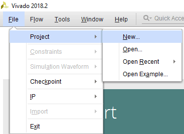
2. From the File menu, select “Project–> New” to create a new project. The “New Project” window will open. Click “Next” to continue.
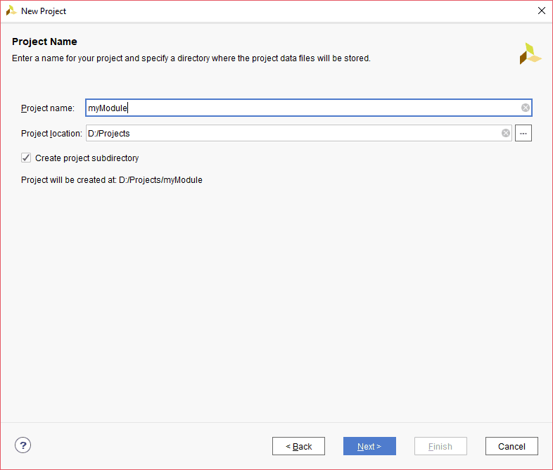
3. Name your project and select a directory to save the project and click “Next” (refer to the picture below).
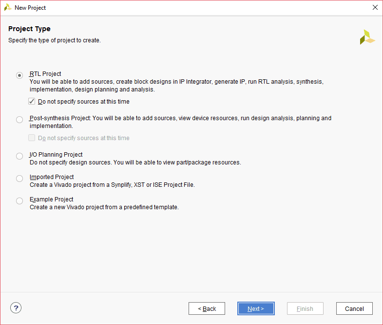
4. In the “Project Type” window, select “RTL Project” and check the “Do not specify sources at this time”. Click “Next”.
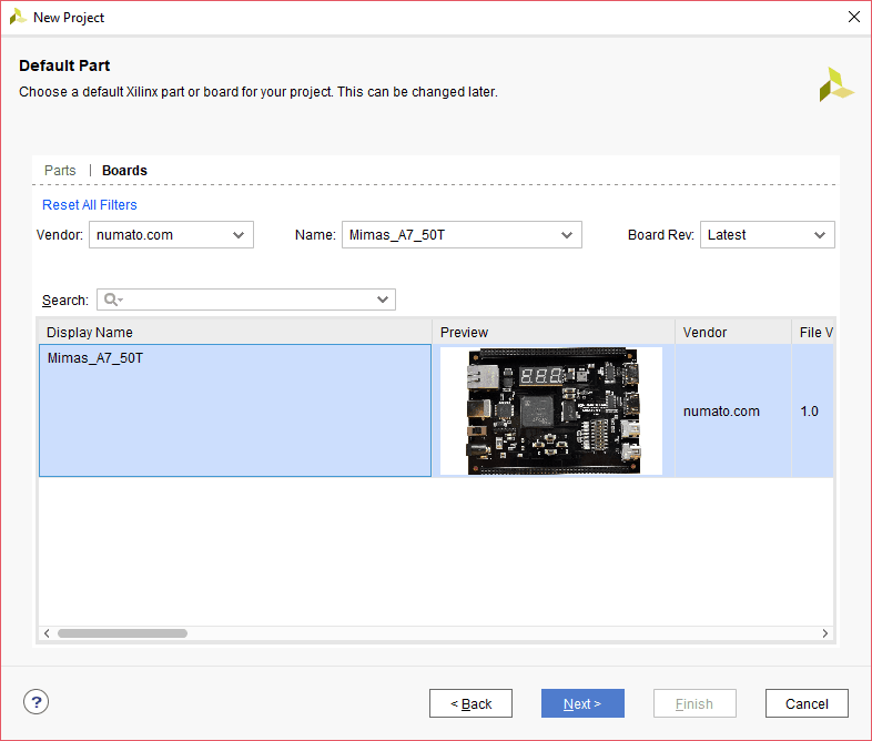
5. In the “Default Part” tab, select “Mimas_A7_50T” from the “Boards” section. If Mimas_A7_50T is not listed, make sure board support files are installed correctly. Click “Next” to proceed.
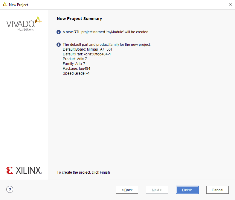
6. Click “Finish” to create a new project.
7. To design a NOT Gate, we have to add sources to the project. To do this, select “Add Sources” under the “Flow Navigator” -> “PROJECT MANAGER” section. Now select “Add or create design sources” and click “Next”.

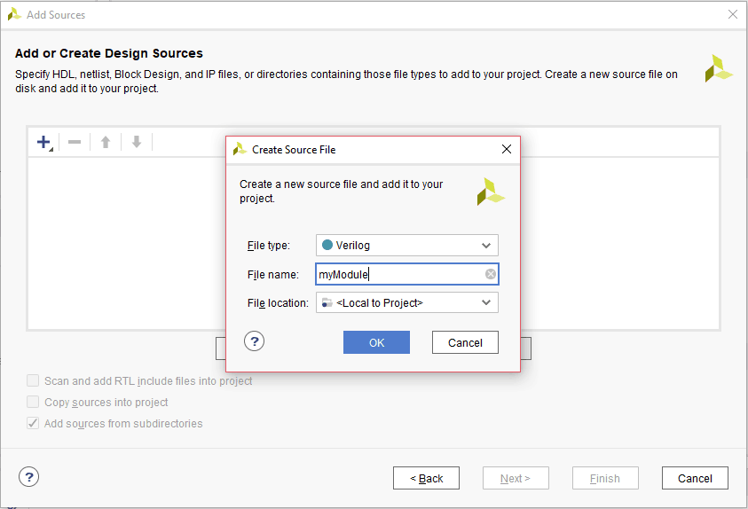
8. Now, select “Create File”. The “Create Source File” window will open, select the “File type” as “Verilog” and give the file name as in the image below. Click “OK” and then click “Finish”.
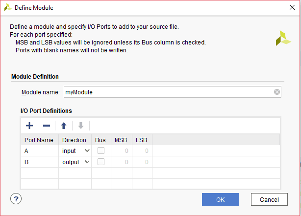
9. The “Define Module” window will open. Now, we have to add the ports required for our project. For our NOT Gate module, we will need only 2 ports. “A” as the input port and “B” as the output port. To add these ports to our project, in the “Define Module” window click on the “+” button to add ports and name the ports and change the direction of the port appropriately. Click “OK”. (refer the image below)
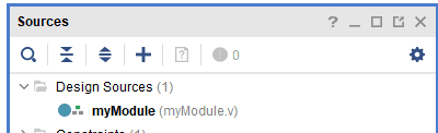
10. The source file myModule.v will be available under “Sources->Design Sources”. Double click on the source file to open it.
11. Now replace the auto-generated module template (or the contents of the whole file) with the code below and save the Verilog source file.
module myModule(A, B);
    input wire A;
    output wire B;
    assign B = !A;
endmodule
Now its time to simulate the code. To run the simulation, we will have to add the simulation sources. To do this, follow the steps below.
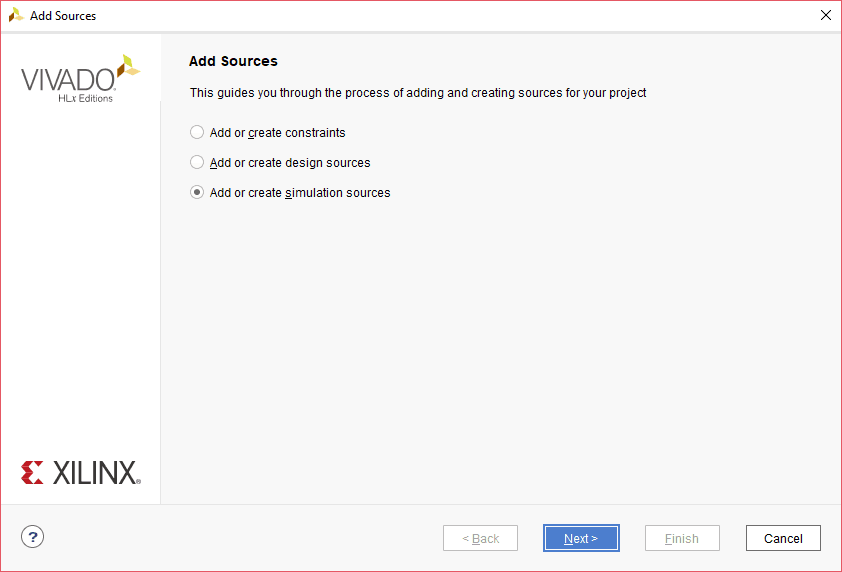
1. Again, select “Add Sources” under the “Flow Navigator” -> “PROJECT MANAGER” section. This time select “Add or create simulation sources” and click “Next”.
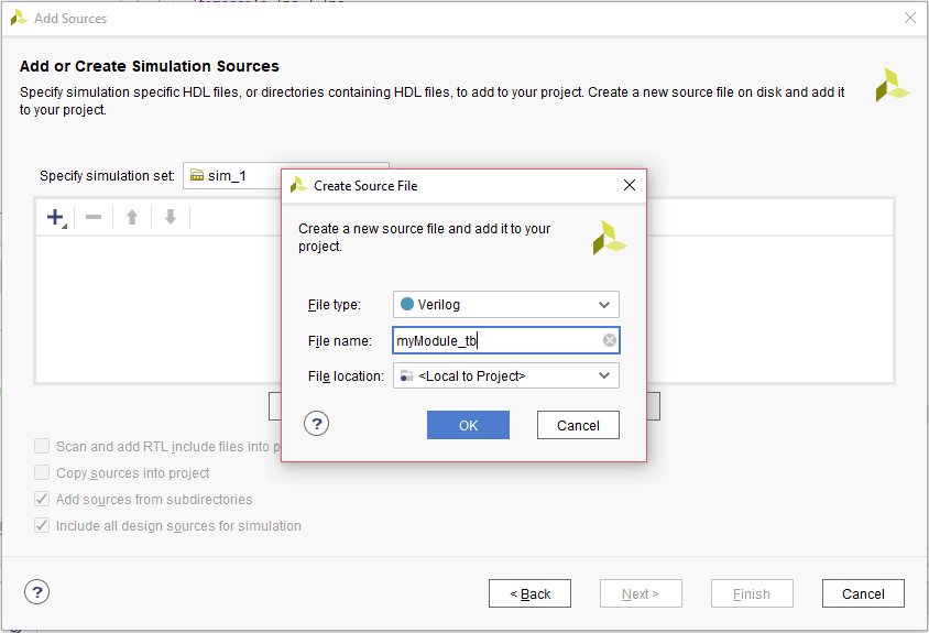
2. Select “Create File”, give the name for the test bench as “myModule_tb” and choose “File type” as “Verilog” as in the image below. Click “OK” then “Finish”.
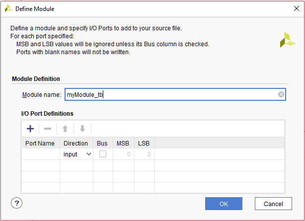
3. A test bench does not need any Inputs and Outputs, so just click “OK” and click “Yes” in the corresponding window that appears.
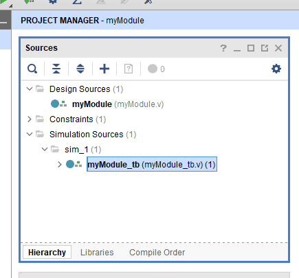
4. Now the test bench will be created under “Sources -> Simulation Sources”.
5. Replace the auto-generated module template with the following code and save it.
module myModule_tb();
wire out;
reg clock;
always begin
#1 clock =!clock;
end
initial begin
//Initialize clock
clock = 0;
//End simulation
#10 $finish;
end
myModule notGate(clock, out);
endmodule
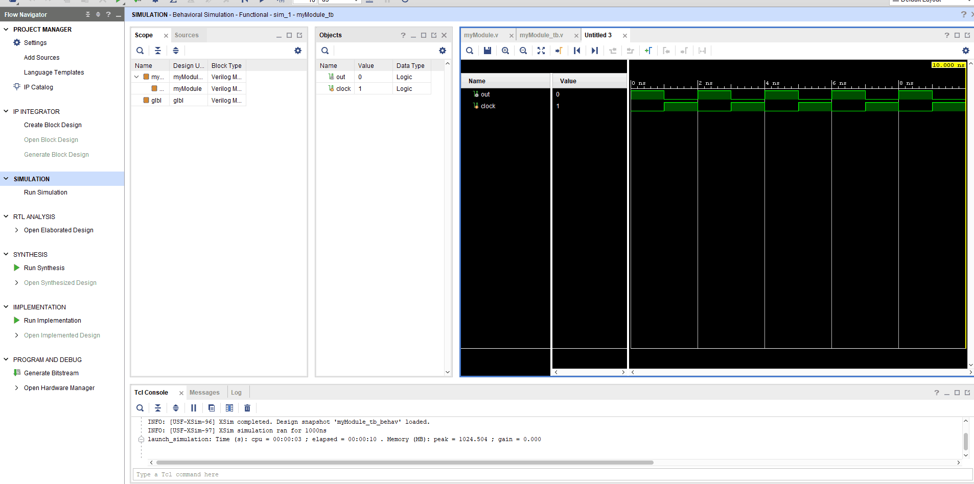
6. Now click on “Run Simulation” –> “Run Behavioral Simulation” under the “Flow Navigator” –> “SIMULATION” panel.
7. Now the built-in simulator will start and you will be presented with a simulation waveform like the one below (Sometimes you may have to zoom in/out a little bit to see the waveform correctly).
Inspect the waveform and make sure that our Verilog module is working as expected. As you can see in the image below, the output is the inverted form of the input clock. This is exactly what we expect from a NOT gate.
In part 4 of this tutorial, we will implement this module on a real hardware.
Download complete Xilinx Vivado simulation project for Mimas A7
Back to part 2 Continue to part 4